SLVAEX9B April 2022 – August 2022 ESD122 , ESD1LIN24-Q1 , ESD204 , ESD224 , ESD2CAN24-Q1 , ESD2CANFD24 , ESD2CANXL24-Q1 , ESD321 , ESD341 , ESD351 , ESD401 , ESD451 , ESD751 , ESD751-Q1 , ESD752 , ESD761 , ESD761-Q1 , ESD762 , ESDS302 , ESDS304 , ESDS312 , ESDS314 , SN65220 , SN65240 , TPD1E01B04 , TPD1E01B04-Q1 , TPD1E04U04 , TPD1E05U06 , TPD1E05U06-Q1 , TPD1E0B04 , TPD1E10B06 , TPD1E10B09-Q1 , TPD1E1B04 , TPD1E6B06 , TPD2E001 , TPD2E001-Q1 , TPD2E007 , TPD2E009 , TPD2E1B06 , TPD2E2U06 , TPD2EUSB30 , TPD2EUSB30A , TPD2S017 , TPD3E001 , TPD3F303 , TPD4E001 , TPD4E001-Q1 , TPD4E002 , TPD4E004 , TPD4E02B04 , TPD4E02B04-Q1 , TPD4E05U06-Q1 , TPD4E101 , TPD4E110 , TPD4E1B06 , TPD4E1U06 , TPD4E6B06 , TPD4F003 , TPD4S009 , TPD4S012 , TPD5E003 , TPD6E001 , TPD6E004 , TPD6E05U06 , TPD8S009 , TSD05 , TSD05C , TSM24A-Q1 , TSM24CA-Q1 , TSM36A , TVS0500 , TVS0701 , TVS1400 , TVS1401 , TVS2200 , TVS2701 , TVS3301 , UC1611-SP , UC2610 , UC3610 , UC3611 , UC3611M
- Abstract
- Trademarks
- 1Definitions of ESD Device Specifications
- 2ESD Layout Tips
-
3ESD Solutions by Package Types
- 3.1 0201 2-pin SON (TI: DPL) | 0.6 mm x 0.3 mm
- 3.2 0402 2-pin SON (TI: DPY) | 1.0 mm × 0.6 mm
- 3.3 2-pin SOD-523 (TI: DYA) | 1.2 mm x 0.8 mm
- 3.4 3-pin SOT-9X3 (TI: DRT) | 1 mm × 1 mm
- 3.5 3-pin SC70 (TI: DCK) | 2 mm × 1.25 mm
- 3.6 3-pin SOT23 (TI:DBZ) | 3.04 mm × 2.64 mm
- 3.7 4-pin SON (TI: DPW) | 0.8 mm × 0.8 mm
- 3.8 5-pin SOT-5X3 (TI: DRL) | 1.6 mm × 1.2 mm
- 3.9 5-pin SOT-23 (TI: DBV) | 2.9 mm × 1.6 mm
- 3.10 6-pin SON (TI: DRY) | 1.45 mm × 1 mm
- 3.11 6-pin SOT-5X3 (TI: DRL) | 1.6 mm × 1.2 mm
- 3.12 6-pin SOT-23 (TI: DBV) | 1.6 mm × 2.9 mm
- 3.13 6-pin SC70 (TI: DCK) | 2.15 mm × 1.4 mm
- 3.14 8-pin SON (TI: DQD) | 1.35 mm × 1.7 mm
- 3.15 10-pin SON (TI: DQA) | 1 mm × 2.5 mm
- 4References
- 5Revision History
2.1 Optimizing Impedance for Dissipating ESD
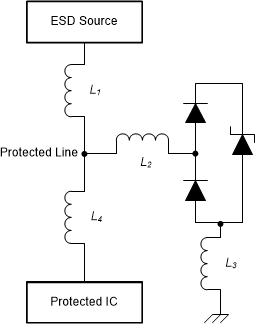
When designing a circuit to dissipate ESD, inductance is an important parasitic to consider. Based on the parasitic inductance, a change in current would cause a change in the overall voltage, destabilizing the overall board performance. Figure 2-1 shows four parasitic inductances between the ESD source and the transient voltage suppressor (TVS) or ESD diodes.
 Figure 2-1 PCB
Inductance Around a Single-Channel TVS
Figure 2-1 PCB
Inductance Around a Single-Channel TVSIn a well-designed system, any inductance is minimized between the ESD source and the path to ground through the TVS. Use the following 5 layout tips to minimize inductance:
- Minimize any inductance between the ESD source and the path to ground through the TVS
- Place the TVS as close to the ESD source or connector as design rules allow
- Place the protected IC much further from the TVS than the TVS is to the connector. Following tips 2 and 3 will ensure L4>>L1, steering the IESD towards TVS. Minimizing L1 is further covered in Section 2.2 and Section 2.3.
- Do not use L2 stubs between the TVS and the protected line. Route directly from the ESD source to the TVS. In a well-designed system, L2 should not be present. Please avoid design practices that introduce inductance between the protected line and the TVS.
- Minimize L3 inductance between the TVS and ground, which is further covered in Section 2.4. This inductance is the most predominant parasitic influencing the overall VESD.