SLVAF10 March   2021 TPS1H000-Q1 , TPS1H100-Q1 , TPS1H200A-Q1 , TPS1HA08-Q1 , TPS1HB08-Q1 , TPS1HB16-Q1 , TPS1HB35-Q1 , TPS1HB50-Q1 , TPS2H000-Q1 , TPS2H160-Q1 , TPS2HB16-Q1 , TPS2HB35-Q1 , TPS2HB50-Q1 , TPS4H000-Q1 , TPS4H160-Q1


  1.   Trademarks
  2. 1Introduction
  3. 2Device Thermals
  4. 3Timing Limitations
    1. 3.1 Background
    2. 3.2 Pulse-Width distortion (PWD)
      1. 3.2.1 Timing Impact of Delay Mismatch
      2. 3.2.2 Power Impact of Delay Mismatch on Resistive Loads
    3. 3.3 Finite Slew Rate
      1. 3.3.1 Timing Impact of Finite Slew Rate and Slew Rate Mismatch
      2. 3.3.2 Impact of Finite Slew Rate on Resistive Load Power
      3. 3.3.3 Impact of Slew Rate on LED Power
  5. 4System-Level Considerations
    1. 4.1 Diagnostics and Protection
      1. 4.1.1 Analog Current Sense
    2. 4.2 Dimming Ratio
    3. 4.3 Side-Stepping Frequency Limitations
  6. 5References

Impact of Finite Slew Rate on Resistive Load Power

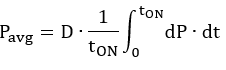
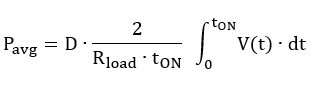
In earlier sections of this report, it was shown that as PWM frequency increases the effects of PWD on load power increases causing significant divergence from the calculated ideal power.

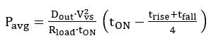
A high side switch's finite slew rate introduces additional challenges that deviates true load power from an ideal case. Unlike PWD, which can either increase or decrease delivered load power, finite slew-rate always results in reduced load power compared to an ideal high side switch as the rise times reduce the time when the full input voltage is present across the load. As frequency increases, the rise and fall times account for more and more of the output ON pulse.

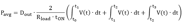
Figure 3-8 defines timing parameters used for analysis.

GUID-DAC70337-36DA-4A0F-869C-4C787CA91019-low.png Figure 3-8 Timing Definition for Resistor Power Analysis
tON is the total duration of the ON cycle pulse.

  • t'ON is the total duration where output is at final voltage
  • tpw(OUT) is the output pulse width
  • trise,fall are rise and fall times calculated from device slew rate, such that
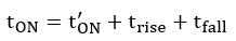
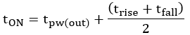
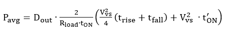
Equation 28. GUID-5ACC5FAE-BC2A-426F-84BF-9690A3358BF7-low.png
Equation 28. GUID-91A8929B-9641-41EC-81C6-32822445C60A-low.png
The average dissipated power in a resistor is R·IAVG2. When considering the slew rate, voltage becomes a linear function of time during rise and fall times. By decomposing the resistor power into the rising, falling, and steady periods of output voltage, we can calculate average load power for an arbitrary resistor with a severely distorted output pulse.
Equation 28. GUID-123D28C9-5E1E-4D38-9A6A-F8F52CFCBAFB-low.png
Equation 28. GUID-CDC330B2-F208-41FC-AC77-A038D8BA476F-low.png
Splitting up the ON cycle waveform yields
Equation 28. GUID-79144B92-3B2E-428D-ABCE-EC5590DA7813-low.png
Even if rise and fall waveforms were complex, it would not be a good use of time to start integrating at this point. As we are assuming the rise and fall periods are linear (constant slew rates), our output waveform is trapezoidal and the power calculation simplifies.

Equation 28. GUID-C3E97ED5-926E-48DC-8D31-CA7A3C9858D3-low.png , where Vvs is the supply voltage. This can be further simplified to:
Equation 28. GUID-AA704914-DAB7-4417-93C8-0AB23783F36A-low.png
As slew rates increase, power dissipated in the resistive load is reduced. At the point where the output only reaches Vvs output power is halved. If frequency is increased further than this point, slew rates will further reduce power as the output will never reach Vvs.