SLVAF10 March   2021 TPS1H000-Q1 , TPS1H100-Q1 , TPS1H200A-Q1 , TPS1HA08-Q1 , TPS1HB08-Q1 , TPS1HB16-Q1 , TPS1HB35-Q1 , TPS1HB50-Q1 , TPS2H000-Q1 , TPS2H160-Q1 , TPS2HB16-Q1 , TPS2HB35-Q1 , TPS2HB50-Q1 , TPS4H000-Q1 , TPS4H160-Q1


  1.   Trademarks
  2. 1Introduction
  3. 2Device Thermals
  4. 3Timing Limitations
    1. 3.1 Background
    2. 3.2 Pulse-Width distortion (PWD)
      1. 3.2.1 Timing Impact of Delay Mismatch
      2. 3.2.2 Power Impact of Delay Mismatch on Resistive Loads
    3. 3.3 Finite Slew Rate
      1. 3.3.1 Timing Impact of Finite Slew Rate and Slew Rate Mismatch
      2. 3.3.2 Impact of Finite Slew Rate on Resistive Load Power
      3. 3.3.3 Impact of Slew Rate on LED Power
  5. 4System-Level Considerations
    1. 4.1 Diagnostics and Protection
      1. 4.1.1 Analog Current Sense
    2. 4.2 Dimming Ratio
    3. 4.3 Side-Stepping Frequency Limitations
  6. 5References

Pulse-Width distortion (PWD)

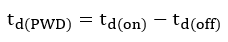
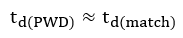
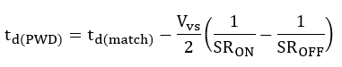
Pulse-width distortion (PWD) arises from mismatch in the HSS’s ON and OFF delay times and low-high/high-low propagation delay. In Figure 3-2, the various timing parameters that need to be considered when implementing a PWM scheme with a TI high-side switch is illustrated. The timing parameters in this diagram are correlated closely to the parameters specified in the "Switching Characteristics" section of the device data sheet. In Figure 3-3, an example excerpt of the switching characterstics can be seen.

GUID-495594E0-A654-423C-AE17-280F98A8251E-low.png Figure 3-2 Pulse-Width Distortion Timing Definition
GUID-676E1FA4-5B46-43B3-AE12-D1A021AC9065-low.png Figure 3-3 TPS4H000-Q1 Timing Parameters
The pulse-width distortion due to propagation-delay effects is defined as
Equation 8. GUID-B048D6B5-32B9-45E9-917E-001F715381F2-low.png
If the high-side switch data sheet specifies td(match), using this parameter is preferable to calculate total distortion as it removes any uncertainty of correlation between slew rate and out. When rise and fall times are much smaller than the pulse width, slew-rate effects can be ignored and total pulse-width distortion may be approximated as:
Equation 9. GUID-E18E07FC-51C5-4351-A5D9-0DEE0432AF9C-low.png
In the case the data sheet does not specify td(match) we can obtain more precision by using:
Equation 8. GUID-F33090E2-6A85-4DFE-A57C-8AFCEA3023D6-low.png
Where Vvs is the high-side supply voltage, and SRON / SROFF are the device turn-on/turn-off slew rates. Note that these specifications are worst-case and are specified at a specific supply voltage and load current. The use of the worst-case parameters will allow us to build a robust design that will work under a wide arrange of ambient conditions.