SNAA320B November 2019 – January 2024 LM4040-N , LM4050-N , LM4120 , LM4128 , LM4128-Q1 , LM4132 , LM4132-Q1 , REF102 , REF1925 , REF1930 , REF1933 , REF1941 , REF20-Q1 , REF200 , REF2025 , REF2030 , REF2033 , REF2041 , REF2125 , REF2912 , REF2920 , REF2925 , REF2930 , REF2933 , REF2940 , REF30 , REF3033-Q1 , REF31-Q1 , REF3112 , REF3120 , REF3125 , REF3130 , REF3133 , REF3140 , REF3212 , REF3212-EP , REF3220 , REF3220-EP , REF3225 , REF3225-EP , REF3230 , REF3230-EP , REF3233 , REF3240 , REF3312 , REF3318 , REF3320 , REF3325 , REF3330 , REF3333 , REF34-Q1 , REF3425 , REF3425-EP , REF3430 , REF3430-EP , REF3433 , REF3433-EP , REF3440 , REF3440-EP , REF3450 , REF35 , REF4132 , REF4132-Q1 , REF50 , REF5020-EP , REF5020A-Q1 , REF5025-EP , REF5025-HT , REF5025A-Q1 , REF5030A-Q1 , REF5040-EP , REF5040A-Q1 , REF5045A-Q1 , REF5050-EP , REF5050A-Q1 , REF50E , REF54 , REF6125 , REF6133 , REF6141 , REF6145 , REF6150 , REF6225 , REF6230 , REF6233 , REF6241 , REF6245 , REF6250 , REF70 , TL431LI , TL432LI , TLV431
5 Calibration
System calibration is often necessary in many signal chain applications to eliminate gain and offset errors. Calibration can remove the voltage reference DC error which reduces the gain error but the amount depends on the calibration method. We can separate calibration into two main calibration categories, single-point calibration and multi-point calibration and this can be seen in Table 5-1.
| SINGLE POINT CALIBRATION | MULTIPOINT CALIBRATION | |
|---|---|---|
| Initial Accuracy | X | X |
| Solder Shift | X | X |
| Thermal Hysteresis | X | X |
| Temperature Drift | X |
Single-point calibration is calibration that is performed at one temperature point. This temperature point is usually either 25C or typical operating temperature of the system. The benefit of this type if calibration is that this calibration can remove voltage reference DC errors post calibration. This type of calibration can be done multiple ways: factory calibration, start-up calibration, run time calibration. Factory calibration is performed at the assembly and test site. In the assembly and test site, the data converter input or output can be compared to a very precise voltage standard. By using the difference between the values, the ADC or microcontroller can store the value internally and adjust the output based on the measured difference. The benefit of this calibration is that measurements can be performed to a high precision and the signal chain system won't need a built-in self test. The drawback is that the calibration cannot be performed at the site of operation, cannot take into account any drift due to aging, and cannot predict the temperature operating conditions of the system. Start-up calibration and run-time calibration are single point calibration tests that are beneficial because these tests can remove the voltage reference DC error at the site of operation. This means that any effect of temperature and aging in the system is taken into account but due to the lack of precise voltage standards, the precision of this calibration can possibly not match the precision of a factory calibration. The inclusion of a built in self test for start-up or run-time calibration possibly requires additional components which can increase the complexity of the system.
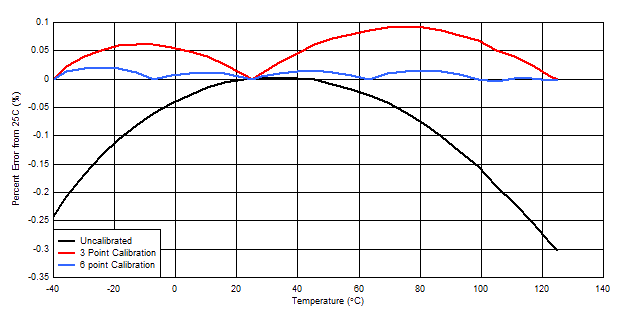
One of the main drawbacks to single-point calibration is that single-point calibration is only valid at a single temperature point and significant temperature variations cause DC errors in the voltage reference that increase the gain error of the data converter. Multi-point calibration is able to fix this draw back because calibration can be performed at multiple temperature points. In Figure 5-1 we can see how much the temperature drift error gets reduced by using a multi-point calibration and creating a temperature profile based on differences that can be used to adjust the final measurements. Typically the gain error correction multiplicatives to the end result of the data conversion. In this example a 3-point calibration decreased the temperature drift error by 3x and a 6 point decreased the error by over 10x. In this example, the final curvature of the 3-point and 6-point calibration lines were created by calculating the slope in between the measured points and then subtracting that result from the uncalibrated value. By knowing the error of the system, a designer can eliminate gain error digitally by multiplying the data converter result by the ratio of (uncalibrated VREF / calibrated VREF).
The temperature calibration is more effective in smaller temperature windows due to this designers must know the operating temperature the device experiences. In Figure 5-1 the uncalibrated waveform is a second order function but this can vary between devices. Getting a first order to higher order curvatures is possible. The temperature drift varies from device to device which can be difficult to calibrate out the error across multiple devices with the same profile so we recommend to calibrate each voltage reference with a unique profile. The drawback of multi-point calibration is the increase of cost, calibration time, and not all temperature curvatures are easy to calibrate. Choosing a more precise voltage reference which better temperature drift to avoid performing multi-point calibration can be attractive.
 Figure 5-1 Temperature Drift Error With
Calibration Profiles
Figure 5-1 Temperature Drift Error With
Calibration ProfilesIn Table 3-2 the temperature drift error is converted into a percent error which is easily comparable to initial accuracy error. Keep in mind that this error is the maximum worst case deviation from 25C in a uncalibrated system. Most devices do not reach a deviation this high. Choosing the device with the lowest temperature drift specification is often more practical in low-resolution systems as temperature calibration can be time consuming and costly. High resolution systems get more complicated because the temperature drift needs to be minimized to maximize the ADC performance especially if the signal chain has signal conditioning components that have their own temperature drift.