SPRACM3E August 2021 – January 2023 F29H850TU , F29H859TU-Q1 , TMS320F280021 , TMS320F280021-Q1 , TMS320F280023 , TMS320F280023-Q1 , TMS320F280023C , TMS320F280025 , TMS320F280025-Q1 , TMS320F280025C , TMS320F280025C-Q1 , TMS320F280033 , TMS320F280034 , TMS320F280034-Q1 , TMS320F280036-Q1 , TMS320F280036C-Q1 , TMS320F280037 , TMS320F280037-Q1 , TMS320F280037C , TMS320F280037C-Q1 , TMS320F280038-Q1 , TMS320F280038C-Q1 , TMS320F280039 , TMS320F280039-Q1 , TMS320F280039C , TMS320F280039C-Q1 , TMS320F280040-Q1 , TMS320F280040C-Q1 , TMS320F280041 , TMS320F280041-Q1 , TMS320F280041C , TMS320F280041C-Q1 , TMS320F280045 , TMS320F280048-Q1 , TMS320F280048C-Q1 , TMS320F280049 , TMS320F280049-Q1 , TMS320F280049C , TMS320F280049C-Q1 , TMS320F28384D , TMS320F28384S , TMS320F28386D , TMS320F28386S , TMS320F28388D , TMS320F28388S , TMS320F28P650DH , TMS320F28P650DK , TMS320F28P650SH , TMS320F28P650SK , TMS320F28P659DH-Q1 , TMS320F28P659DK-Q1 , TMS320F28P659SH-Q1
- Using the Fast Serial Interface (FSI) With Multiple Devices in an Application
- Trademarks
- 1Introduction to the FSI Module
- 2FSI Applications
- 3Handshake Mechanism
- 4Sending and Receiving FSI Data Frames
- 5Daisy-Chain Topology Tests
- 6Star Topology Tests
-
7Event Synchronization Over FSI
- 7.1 Introduction
- 7.2 C2000Ware FSI EPWM Sync Examples
- 7.3 Additional Tips and Usage of FSI Event Sync
- 8References
- 9Revision History
5.2.2.1.1 CPU/DMA control
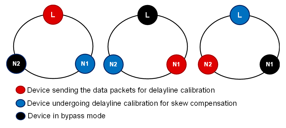
Device 2 delayline calibration: The Device 1 calls the Device 2 using the assigned ID and once the Device 2 receives the calibration call, it uses the data packets sent by Device 1 to calibrate its delaylines. The Device 3, while in by-pass mode, transmits the packet received from the Device 2 to the Device 1 using CPU control.
Device 3 delayline calibration: The Device 2 calls the Device 3 using the assigned ID and once the Device 3 receives the calibration call, it uses the data packets sent by Device 2 to calibrate its delaylines. The Device 1, while in by-pass mode, transmits the packet received from the Device 3 to the Device 2 using CPU control.
Device 1 delayline calibration: The Device 3 calls the Device 1 using the assigned ID and once the Device 1 receives the calibration call, it uses the data packets sent by Device 3 to calibrate its delaylines. The Device 2, while in by-pass mode, transmits the packet received from the Device 1 to the Device 3 using CPU control.
All the three devices are thus calibrated in a phased manner as shown in the figure Figure 5-13 and by the end of calibration the Rx delaylines of all the devices in the daisy chain are configured with appropriate values.
 Figure 5-13 Calibration Diagram of Delay
Lines for Skew Compensation in CPU, DMA Control