SPRACM3E August 2021 – January 2023 TMS320F280021 , TMS320F280021-Q1 , TMS320F280023 , TMS320F280023-Q1 , TMS320F280023C , TMS320F280025 , TMS320F280025-Q1 , TMS320F280025C , TMS320F280025C-Q1 , TMS320F280033 , TMS320F280034 , TMS320F280034-Q1 , TMS320F280036-Q1 , TMS320F280036C-Q1 , TMS320F280037 , TMS320F280037-Q1 , TMS320F280037C , TMS320F280037C-Q1 , TMS320F280038-Q1 , TMS320F280038C-Q1 , TMS320F280039 , TMS320F280039-Q1 , TMS320F280039C , TMS320F280039C-Q1 , TMS320F280040-Q1 , TMS320F280040C-Q1 , TMS320F280041 , TMS320F280041-Q1 , TMS320F280041C , TMS320F280041C-Q1 , TMS320F280045 , TMS320F280048-Q1 , TMS320F280048C-Q1 , TMS320F280049 , TMS320F280049-Q1 , TMS320F280049C , TMS320F280049C-Q1 , TMS320F28384D , TMS320F28384S , TMS320F28386D , TMS320F28386S , TMS320F28388D , TMS320F28388S , TMS320F28P650DH , TMS320F28P650DK , TMS320F28P650SH , TMS320F28P650SK , TMS320F28P659DH-Q1 , TMS320F28P659DK-Q1 , TMS320F28P659SH-Q1
- Using the Fast Serial Interface (FSI) With Multiple Devices in an Application
- Trademarks
- 1Introduction to the FSI Module
- 2FSI Applications
- 3Handshake Mechanism
- 4Sending and Receiving FSI Data Frames
- 5Daisy-Chain Topology Tests
- 6Star Topology Tests
-
7Event Synchronization Over FSI
- 7.1 Introduction
- 7.2 C2000Ware FSI EPWM Sync Examples
- 7.3 Additional Tips and Usage of FSI Event Sync
- 8References
- 9Revision History
5.2.1 CPU/DMA Control
-
Test condition
Device 1 sends data -> Device 2 receives data -> Device 2 moves RX data to TX buffer and sends data to Device 3->…..-> Device 3 moves RX data to TX buffer and sends data to Device 1 -> Device1 receives data and verifies the data matches the originally sent TX data.
-
Test case
Data length of 8 words, 1 data line, TXCLK = 50 MHz, with setting ① for CPU control case and ② for DMA control case (Table 5-1) enabled.
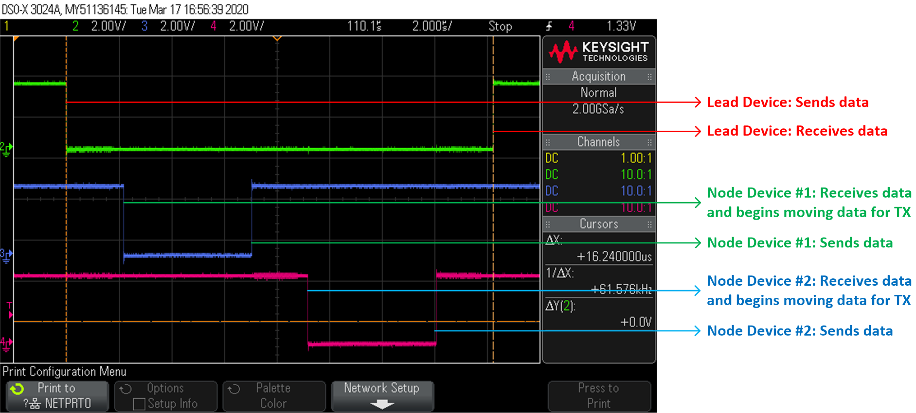
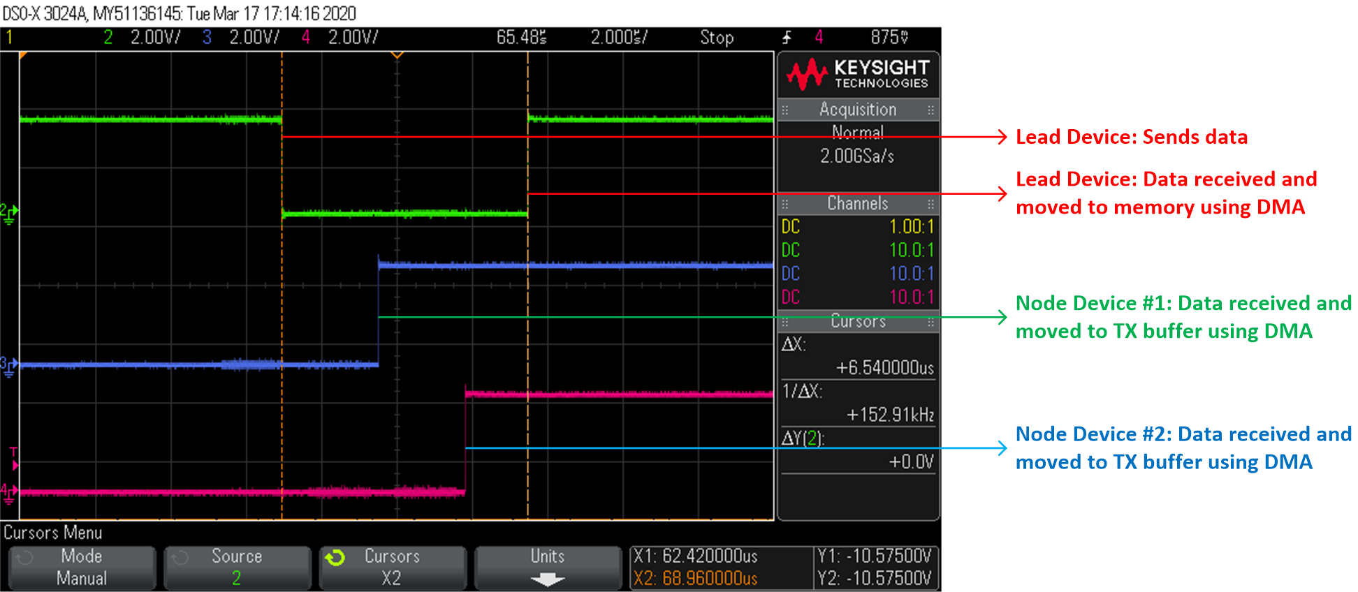
In the tests, GPIOs are toggled within software when specific events occur during the communication and measured using an oscilloscope to obtain the respective timing data. In the figures below, the green signal represents the GPIO toggling of Device 1 (Lead device), the blue signal represents the GPIO toggling of Device 2 (Node device), and the magenta signal represents the GPIO toggling of Device 3 (Node device).
 Figure 5-7 FSI Communication With CPU
Control Among Three Devices
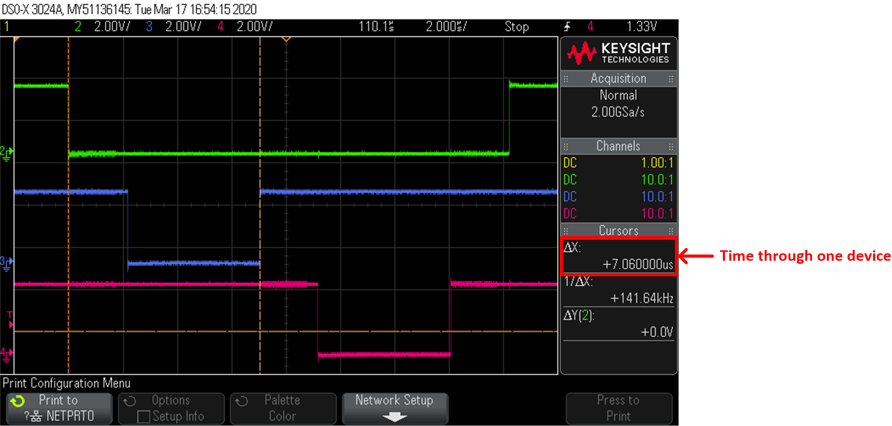
 Figure 5-8 Time of Data Going Through One
Device - CPU Control
Figure 5-8 Time of Data Going Through One
Device - CPU ControlFor the CPU control case, the time needed for the data transmission to complete the three device daisy-chain loop is 16.2 µs, as shown in Figure 5-7. This time will increase by 7.1 us for each device added to the daisy-chain connection system, as shown in Figure 5-8. The 7.1 µs increased time per device includes the time for transmission and moving RX data to the TX buffer and registers.
 Figure 5-9 FSI Communication With DMA
Control Among Three Devices
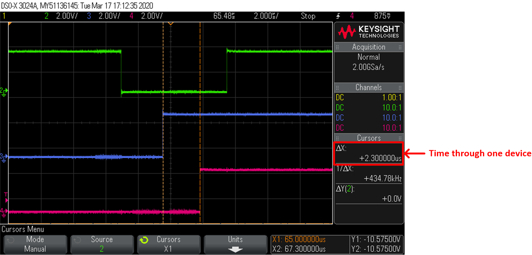
 Figure 5-10 Time of Data Going Through One
Device - DMA Control
Figure 5-10 Time of Data Going Through One
Device - DMA ControlFor the DMA control case, the time needed for the data transmission to complete the three device daisy-chain loop is 6.5 µs, as shown in Figure 5-9. This time will increase by 2.3 us for each device added to the daisy-chain connection system, as shown in Figure 5-10. The 2.3 µs increased time per device includes the time for transmission and moving RX data to the TX buffer and registers.