SPRACZ1 October 2021 F29H850TU , F29H859TU-Q1 , TMS320F280021 , TMS320F280021-Q1 , TMS320F280023 , TMS320F280023-Q1 , TMS320F280023C , TMS320F280025 , TMS320F280025-Q1 , TMS320F280025C , TMS320F280025C-Q1 , TMS320F280040-Q1 , TMS320F280040C-Q1 , TMS320F280041 , TMS320F280041-Q1 , TMS320F280041C , TMS320F280041C-Q1 , TMS320F280045 , TMS320F280048-Q1 , TMS320F280048C-Q1 , TMS320F280049 , TMS320F280049-Q1 , TMS320F280049C , TMS320F280049C-Q1 , TMS320F28044 , TMS320F28075 , TMS320F28075-Q1 , TMS320F28076 , TMS320F28374D , TMS320F28374S , TMS320F28375D , TMS320F28375S , TMS320F28375S-Q1 , TMS320F28376D , TMS320F28376S , TMS320F28377D , TMS320F28377D-EP , TMS320F28377D-Q1 , TMS320F28377S , TMS320F28377S-Q1 , TMS320F28378D , TMS320F28378S , TMS320F28379D , TMS320F28379D-Q1 , TMS320F28379S , TMS320F28384D , TMS320F28384D-Q1 , TMS320F28384S , TMS320F28384S-Q1 , TMS320F28386D , TMS320F28386D-Q1 , TMS320F28386S , TMS320F28386S-Q1 , TMS320F28388D , TMS320F28388S , TMS320F28P650DH , TMS320F28P650DK , TMS320F28P650SH , TMS320F28P650SK , TMS320F28P659DH-Q1 , TMS320F28P659DK-Q1 , TMS320F28P659SH-Q1
1 Introduction
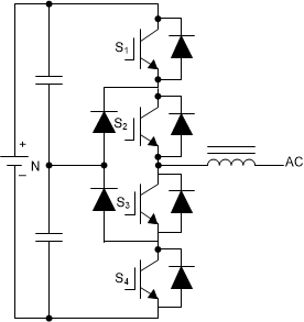
Figure 1-1 shows a typical single phase three-level I-Type inverter, named neutral point clamped (NPC) inverter. The single phase NPC inverter includes 4 FETs, like IGBT, in series, where S1 and S4 are called outer switches, with S2 and S3 called inner switches.
 Figure 1-1 Single Phase Three-Level I-Type
Inverter
Figure 1-1 Single Phase Three-Level I-Type
InverterConsidering the difference between positive cycle and negative cycle when tied to the grid, the general switching states of four FETs in normal operation are shown in Table 1-1.
| Symbol | Switching states | |||
|---|---|---|---|---|
| S1 | S2 | S3 | S4 | |
| Positive | Alternate switch | Remaining ON | Alternate switch | Remaining OFF |
| Negative | Remaining OFF | Alternate switch | Remaining ON | Alternate switch |
There are several events which lead to quick shut-down to protect the semiconductors and the system, like over current, thermal overload, etc. Unlike immediately switching off all the FETs simultaneously in two level inverter, for three-level inverter, it must be made sure that the correct switch-off sequence is maintained: outer switches (S1 or S4) off first, inner switches (S2 or S3) off after a specific delay, while the inner one must be switched on firstly during the recover process. This delayed protection requirement has been a challenge for lots of UPS or solar inverter customers for a long time. Since using software algorithms will cause too much delay to provide in-time protection, some customers have to use external hardware circuits, like FPGA or CPLD, to achieve such protection logic, which increases the system cost and also the development effort.
This application report demonstrates how to implement delayed protection with existed Type 4 ePWM features that are available in all new C2000 devices, including F2838xD/S, F2837xD/S, F2807x and F28004x. In the Type 4 EPWM module, the Action Qualifier sub-module includes two additional trigger events (T1 and T2), which can be sourced from comparator, trip or sync events, together with Dead-Band sub-module, make it possible to add customized delay time to tripped/fault signals.