SPRACZ1 October 2021 F29H850TU , F29H859TU-Q1 , TMS320F280021 , TMS320F280021-Q1 , TMS320F280023 , TMS320F280023-Q1 , TMS320F280023C , TMS320F280025 , TMS320F280025-Q1 , TMS320F280025C , TMS320F280025C-Q1 , TMS320F280040-Q1 , TMS320F280040C-Q1 , TMS320F280041 , TMS320F280041-Q1 , TMS320F280041C , TMS320F280041C-Q1 , TMS320F280045 , TMS320F280048-Q1 , TMS320F280048C-Q1 , TMS320F280049 , TMS320F280049-Q1 , TMS320F280049C , TMS320F280049C-Q1 , TMS320F28044 , TMS320F28075 , TMS320F28075-Q1 , TMS320F28076 , TMS320F28374D , TMS320F28374S , TMS320F28375D , TMS320F28375S , TMS320F28375S-Q1 , TMS320F28376D , TMS320F28376S , TMS320F28377D , TMS320F28377D-EP , TMS320F28377D-Q1 , TMS320F28377S , TMS320F28377S-Q1 , TMS320F28378D , TMS320F28378S , TMS320F28379D , TMS320F28379D-Q1 , TMS320F28379S , TMS320F28384D , TMS320F28384D-Q1 , TMS320F28384S , TMS320F28384S-Q1 , TMS320F28386D , TMS320F28386D-Q1 , TMS320F28386S , TMS320F28386S-Q1 , TMS320F28388D , TMS320F28388S , TMS320F28P650DH , TMS320F28P650DK , TMS320F28P650SH , TMS320F28P650SK , TMS320F28P659DH-Q1 , TMS320F28P659DK-Q1 , TMS320F28P659SH-Q1
2.4 Auxiliary EPWM Output Configuration
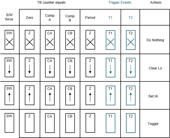
The main challenge is how to insert a customized delay for the tripped action at the specific EPWM output, which is EPWM2B during positive cycle and EPWM1B during negative cycle in this example. As shown in Figure 2-2 with the latest Type 4 EPWM, events T1 and T2, sourcing from comparator, trip or sync events, can also generate actions through Action Qualifier submodule, which mean that dead-band insertion for trip events is possible. Considering the ease of configuration, an extra EPWM7A will be used as auxiliary trip signal for EPWM1B or EPWM2B.
 Figure 2-2 Action-Qualifier Actions for
EPWMxA and EPWMxB Outputs
Figure 2-2 Action-Qualifier Actions for
EPWMxA and EPWMxB OutputsThe detailed configurations can refer to the library function initEPWM_aux_trip(uint32_t aux_pwm_base, EPWM_DigitalCompareTripInput system_trip_source, uint16_t trip_delay). By default, EPWM7A keeps low during normal operation, while it outputs high when the trip signal occurs. The customized delay is defined for the rising edge using the dead-band module with the below settings, and the initial delay is set with trip_delay=1 µs, which could be adjusted in actual applications. Besides, after the trip signal disappears, EPWM7A is expected to turn low immediately, and then wait for the next trip event. The dead-band settings are as below.
    // S1 = 1
    EPWM_setDeadBandDelayMode(aux_pwm_base,EPWM_DB_RED, true);
    // S2 = 0
    EPWM_setDeadBandDelayPolarity(aux_pwm_base, EPWM_DB_RED, EPWM_DB_POLARITY_ACTIVE_HIGH);
    // S4 = 0
    EPWM_setRisingEdgeDeadBandDelayInput(aux_pwm_base, EPWM_DB_INPUT_EPWMA);
    EPWM_setRisingEdgeDelayCount(aux_pwm_base, trip_delay);
Before the action-qualifier settings, it is required to configure the trip signal (active low) and the recover signal (active high) as DCBEVT1 and DCBEVT2, which are set as T1 and T2 events for EPWM7A, respectively. With the system trip source signal defined in Section 2.2, the related codes are as shown below:
    // DCBH = TRIPIN4 = INPUT X-BAR 1 = EPWM8A in this example
    EPWM_selectDigitalCompareTripInput(aux_pwm_base, system_trip_source, EPWM_DC_TYPE_DCBH);
     //Trigger DCBEVT1 when system_trip_source signal goes low(fault occurs)
    //Trigger DCBEVT2 when system_trip_source signal goes high(recover from fault)
    EPWM_setTripZoneDigitalCompareEventCondition(aux_pwm_base,EPWM_TZ_DC_OUTPUT_B1,   EPWM_TZ_EVENT_DCXH_LOW);
    EPWM_setTripZoneDigitalCompareEventCondition(aux_pwm_base,EPWM_TZ_DC_OUTPUT_B2,  EPWM_TZ_EVENT_DCXH_HIGH);
    //
    // DCBEVT1/2 event as AQ T1/2
    // T1 = DCBEVT1
    EPWM_setActionQualifierT1TriggerSource(aux_pwm_base, EPWM_AQ_TRIGGER_EVENT_TRIG_DCB_1);
    // T2 = DCBEVT2
    EPWM_setActionQualifierT2TriggerSource(aux_pwm_base, EPWM_AQ_TRIGGER_EVENT_TRIG_DCB_2);
Then, the auxiliary EPWM output EPWM7A is controlled to set high at T1 event and clear low at T2 event through the action-qualifier submodule.
    EPWM_setActionQualifierAction(aux_pwm_base,
                                  EPWM_AQ_OUTPUT_A, EPWM_AQ_OUTPUT_HIGH,
                                  EPWM_AQ_OUTPUT_ON_T1_COUNT_UP);
    EPWM_setActionQualifierAction(aux_pwm_base,
                                  EPWM_AQ_OUTPUT_A, EPWM_AQ_OUTPUT_HIGH,
                                  EPWM_AQ_OUTPUT_ON_T1_COUNT_DOWN);
    EPWM_setActionQualifierAction(aux_pwm_base,
                                  EPWM_AQ_OUTPUT_A, EPWM_AQ_OUTPUT_LOW,
                                  EPWM_AQ_OUTPUT_ON_T2_COUNT_UP);
    EPWM_setActionQualifierAction(aux_pwm_base,
                                  EPWM_AQ_OUTPUT_A, EPWM_AQ_OUTPUT_LOW,
                                  EPWM_AQ_OUTPUT_ON_T2_COUNT_DOWN);