SPRAD15 March 2022 F29H850TU , F29H859TU-Q1 , TMS320F280021 , TMS320F280021-Q1 , TMS320F280023 , TMS320F280023-Q1 , TMS320F280023C , TMS320F280025 , TMS320F280025-Q1 , TMS320F280025C , TMS320F280025C-Q1 , TMS320F280033 , TMS320F280034 , TMS320F280034-Q1 , TMS320F280036-Q1 , TMS320F280036C-Q1 , TMS320F280037 , TMS320F280037-Q1 , TMS320F280037C , TMS320F280037C-Q1 , TMS320F280038-Q1 , TMS320F280038C-Q1 , TMS320F280039 , TMS320F280039-Q1 , TMS320F280039C , TMS320F280039C-Q1 , TMS320F280040-Q1 , TMS320F280040C-Q1 , TMS320F280041 , TMS320F280041-Q1 , TMS320F280041C , TMS320F280041C-Q1 , TMS320F280045 , TMS320F280048-Q1 , TMS320F280048C-Q1 , TMS320F280049 , TMS320F280049-Q1 , TMS320F280049C , TMS320F280049C-Q1 , TMS320F28075 , TMS320F28075-Q1 , TMS320F28076 , TMS320F28374D , TMS320F28375D , TMS320F28376D , TMS320F28377D , TMS320F28377D-EP , TMS320F28377D-Q1 , TMS320F28378D , TMS320F28379D , TMS320F28379D-Q1 , TMS320F28384D , TMS320F28384D-Q1 , TMS320F28384S , TMS320F28384S-Q1 , TMS320F28386D , TMS320F28386D-Q1 , TMS320F28386S , TMS320F28386S-Q1 , TMS320F28388D , TMS320F28388S , TMS320F28P550SG , TMS320F28P550SJ , TMS320F28P559SG-Q1 , TMS320F28P559SJ-Q1 , TMS320F28P650DH , TMS320F28P650DK , TMS320F28P650SH , TMS320F28P650SK , TMS320F28P659DH-Q1 , TMS320F28P659DK-Q1 , TMS320F28P659SH-Q1
2.2 Secondary Side
With an increasing requirement for higher efficiency in LLC topology, synchronous rectification is becoming a must-have. Traditionally, it is difficult for an MCU to handle a multi-phase synchronous rectification topology, given the complex timing between the primary and secondary side, and between phases. However, the flexible type-4 PWM is making it possible with C2000.
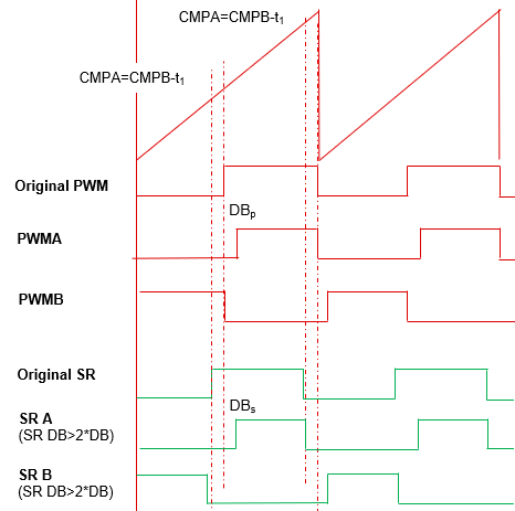
Figure 2-5 shows the PWM configuration of synchronized rectification (SR) MOS. Note SR is using a separate PWM module from the primary side, thus a new set of CMPAs and CMPBs could be used with new action qualifier events. In order to ensure the safe operation of SR FETs, SR FETs are set to switch off slightly earlier than primary side FETs by setting CMPAS = CMPAP-t1 and CMPBS= CMPBP- t1. Meanwhile, the corresponding SR should also switch on later than the primary side switch, thus an AHC mode is used to delay the rising edge of the original SR signal to generate the PWM of SRA and complementary SRB. Considering a dead-band is existing in primary-side PWM, the dead-band on the secondary side must be large enough to make sure the SRx does not switch earlier than the primary side:
DBs>t1+DBp
To make the calculation easier, we could set t1= DBp, thus:
DBs>2*DBp
 Figure 2-5 SR MOS PWM
Configuration