SSZT741 april 2018 UCC27710 , UCC27712 , UCC27734 , UCC27734-Q1 , UCC27735 , UCC27735-Q1
I recently moved to a new apartment, so I decided to go shopping for a vacuum cleaner. As I walked around the appliances section, I noticed how many of the vacuums were cordless. The manufacturers also seemed to be advertising more suction power, longer battery life and extended warranties.
One takeaway, as a customer, was that robust and reliable solutions are facilitating longer lifetimes, which in return improve a product’s reputation. This is relevant for applications like small home appliances, garden and power tools, and residential air conditioners that use electric motors. Most of these systems use DC drives such as brushed-DC (BDC) motors, three-phase brushless-DC (BLDC) motors or stepper drives. Given their high efficiency, lower audible noise and longer life spans, BLDC motors are widely used in appliances in order to achieve longer battery life, reduce cooling efforts and enable reliable operation.
Electronic motor control represents one of the main applications for MOSFET drivers. When selecting a gate driver for your DC drives, there are some design considerations to keep in mind in order to achieve higher system robustness. Part 1 of this blog series will cover negative voltage handling.
Negative voltage, in relation to a gate driver, it is the ability to withstand voltages seen at the input and output. Negative voltages result from parasitic inductances caused by switching transitions, leakage or poor layout. These unwanted voltages commonly appear in applications like motor drives, appliances and switch-mode power supplies.
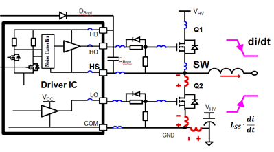
Of all the issues resulting from parasitic inductances, one of the main problems for motor control is a tendency for the switch node (HS) to undershoot the ground following switching transitions. Figure 1 shows the internal parasitic inductances and board-layout inductances that exist in any design.
Figure 1 also shows that during the high-side turn-off, with continuous current flowing in the inductor, as the high-side current falls the low-side current rises. In most cases, this occurs in the body diode for a short period of time. The current in the parasitic inductance generates a negative voltage relative to the MOSFET channel and body diode. The result is a negative voltage spike on HS, which can cause gate driver malfunction, DBOOT diode overcurrent or VHB-HS overvoltage.
 Figure 1 Negative Voltage on HS: Di/dt
Effect on a Gate Driver
Figure 1 Negative Voltage on HS: Di/dt
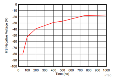
Effect on a Gate DriverIt’s important for gate drivers to have significant HS-negative voltage capabilities in order to improve robustness in your designs. For example, the UCC27710 600V driver maintains the correct output state within the voltage and time conditions shown in Figure 2. With a negative voltage capability of -11VDC across temperature, this solution offers robust operation under these conditions, which is critical for a reliable solution.
 Figure 2 UCC27710 HS-negative Voltage
Capability
Figure 2 UCC27710 HS-negative Voltage
CapabilityNow, let’s discuss how to reduce those unwanted negative spikes. The parasitic inductances mainly come from the board layout. The layout of half-bridge power devices can be relatively tight, but what about the long trace from the FET to the bulk input capacitor?
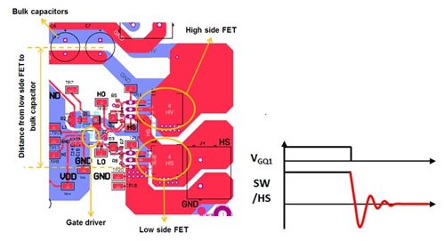
Figure 3 shows a typical half-bridge driver and power-train layout. You can see that the MOSFETs are relatively close together, but due to PCB board size constraints, the bulk capacitor is often placed further from the FETs. This board layout path will result in source-to-capacitor parasitic inductance, which can result in large negative HS spikes.
 Figure 3 Board Layout Path Resulting in
Parasitic Inductance
Figure 3 Board Layout Path Resulting in
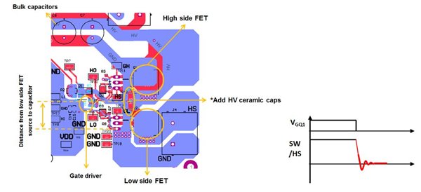
Parasitic InductanceFigure 4 shows the bottom layer of the board layout. If you add high-voltage ceramic capacitors, you can place them very close to the power MOSFETs. Now the path from the low-side FET source to the capacitor is reduced significantly. Assuming that the parasitic inductance is relative to the path length, you can reduce the negative spike, as Figure 4 illustrates.
 Figure 4 Improved Board Layout
Resulting in a Reduced Negative Spike
Figure 4 Improved Board Layout
Resulting in a Reduced Negative SpikeAs you can see, negative voltage handling is a critical function for gate drivers. Keep this in mind to achieve higher system robustness when designing motor-drive applications.
Additional Resources
- These designs from the TI Designs reference designs library showcase robust gate drivers in DC drive and appliance subsystems:
- 230-V, 400-W 92% Efficiency Battery Charger with PFC and LLC for 36V Power Tools Reference Design.
- Electronically Commutated Motor Reference Design for HVAC Blowers with Low BOM Cost.
- 480W, 97% n Efficiency, Ultra-Compact (480W/in3), Bidirectional DC/DC Reference Design.
- 230V, 3.5kW PFC with >98% Efficiency Optimized for BOM and Size Reference Design.