SWRU546E October   2018  – May 2022 AWR6843 , AWR6843AOP , IWR6443 , IWR6843 , IWR6843AOP


  1.   Trademarks
  2. 1Getting Started
    1. 1.1 Introduction
    2. 1.2 Key Features
      1. 1.2.1 Summary of Features
      2. 1.2.2 xWR6843ISK
      3. 1.2.3 IWR6843ISK-ODS (Overhead Detection Sensing)
      4. 1.2.4 IWR6843AOP
      5. 1.2.5 MMWAVEICBOOST
    3. 1.3 What’s Included
      1. 1.3.1 Kit Contents
        1. 1.3.1.1 xWR6843ISK
        2. 1.3.1.2 IWR6843ISK-ODS
        3. 1.3.1.3 IWR6843AOPEVM
        4. 1.3.1.4 MMWAVEICBOOST
  3. 2MMWAVEICBOOST
    1. 2.1 Hardware
    2. 2.2 Block Diagram and Features
      1. 2.2.1 Block Diagram
      2. 2.2.2 Hardware Features
    3. 2.3 Muxing Scheme for Multiple Sources
    4. 2.4 Using the MMWAVEICBOOST With the Starter Kit
      1. 2.4.1 PC Connection
      2. 2.4.2 Flashing the QSPI Flash on the Antenna Module
      3. 2.4.3 MMWAVEICBOOST and Antenna Module Connections for Modular Testing
    5. 2.5 Interfacing with the DCA1000EVM
      1. 2.5.1 mmWave Studio Interface
      2. 2.5.2 MMWAVEICBOOST and Antenna Module Configuration
      3. 2.5.3 DCA1000 EVM Connection
    6. 2.6 Power Connections
    7. 2.7 Connectors
      1. 2.7.1 20-Pin LaunchPad and Booster Pack Connectors (J5, J6)
      2. 2.7.2 60-Pin High Density (HD) Connector (J4 and J17)
      3. 2.7.3 60-Pin High Density (HD) Connector (J10)
      4. 2.7.4 MIPI 60-Pin Connector (J9)
      5. 2.7.5 TI 14-Pin JTAG Connector (J19)
      6. 2.7.6 CAN Connector (J1 and J2)
      7. 2.7.7 Ultra-Miniature Coaxial Connector (J3)
    8. 2.8 Jumpers, Switches and LEDs
      1. 2.8.1 Sense on Power (SOP) Jumpers
      2. 2.8.2 I2C Connections
        1. 2.8.2.1 Default I2C Address
        2. 2.8.2.2 43
        3. 2.8.2.3 3.3-V Rail Options
        4. 2.8.2.4 Miscellaneous Headers
        5. 2.8.2.5 Switches and LEDs
          1. 2.8.2.5.1 Switches
  4. 3xWR6843ISK / IWR6843ISK-ODS REV C
    1. 3.1  Hardware
      1. 3.1.1 xWR6843ISK EVM
      2. 3.1.2 IWR6843ISK-ODS EVM
    2. 3.2  xWR6843ISK/IWR6843ISK-ODS Block Diagram
    3. 3.3  PCB Storage and Handling Recommendations
    4. 3.4  Power Connections
      1. 3.4.1 Higher Power Applications
    5. 3.5  Interfaces
      1. 3.5.1 Switches, Buttons and Muxes
      2. 3.5.2 List of LEDs
      3. 3.5.3 CANFD
      4. 3.5.4 I2C Connections
        1. 3.5.4.1 EEPROM
        2. 3.5.4.2 Default I2C Address
    6. 3.6  xWR6843ISK Antenna
    7. 3.7  IWR6843ISK-ODS Antenna
    8. 3.8  Modular Mode
    9. 3.9  DCA1000EVM Mode
    10. 3.10 MMWAVEICBOOST Mode
  5. 4xWR6843AOPEVM Rev G
    1. 4.1  Hardware
    2. 4.2  Block Diagram
    3. 4.3  PCB Storage and Handling Recommendations
    4. 4.4  Heat Sink and Temperature
    5. 4.5  xWR6843AOPEVM Antenna
    6. 4.6  Switch Settings
    7. 4.7  xWR6843AOPEVM Muxing Scheme
      1. 4.7.1 SOP Configuration
    8. 4.8  Modular, DCA1000EVM and MMWAVEICBOOST Mode
      1. 4.8.1 Modular Mode
      2. 4.8.2 DCA1000EVM Mode
      3. 4.8.3 MMWAVEICBOOST Mode
    9. 4.9  Known Issues: Spurious Performance
    10. 4.10 PC Connection
      1. 4.10.1 Installing the Drivers
      2. 4.10.2 Flashing the Board
    11. 4.11 REACH Compliance
    12. 4.12 Regulatory Statements with Respect to the xWR6843AOPEVM Rev G
  6. 5xWR6843AOPEVM Rev F
    1. 5.1  Hardware
    2. 5.2  Block Diagram
    3. 5.3  PCB Storage and Handling Recommendations
    4. 5.4  Heat Sink and Temperature
    5. 5.5  xWR6843AOPEVM Antenna
    6. 5.6  Switch Settings
    7. 5.7  xWR6843AOPEVM Muxing Scheme
      1. 5.7.1 SOP Configuration
    8. 5.8  Modular and MMWAVEICBOOST Mode
      1. 5.8.1 Modular Mode
      2. 5.8.2 MMWAVEICBOOST Mode
    9. 5.9  PC Connection
      1. 5.9.1 Installing the Drivers
      2. 5.9.2 Flashing the Board
      3. 5.9.3 DCA1000
    10. 5.10 REACH Compliance
  7. 6IWR6843ISK / IWR6843ISK-ODS (deprecated)
    1. 6.1 Hardware
      1. 6.1.1 IWR6843ISK EVM
      2. 6.1.2 IWR6843ISK-ODS EVM
    2. 6.2 IWR6843ISK/IWR6843ISK-ODS Block Diagram
    3. 6.3 PCB Storage and Handling Recommendations
    4. 6.4 Power Connections
    5. 6.5 Miscellaneous and LEDs
      1. 6.5.1 List of LEDs
      2. 6.5.2 I2C Connections
        1. 6.5.2.1 EEPROM
        2. 6.5.2.2 Default I2C Address
    6. 6.6 IWR6843ISK Antenna
    7. 6.7 IWR6843ISK-ODS Antenna
  8. 7IWR6843AOPEVM (Deprecated)
    1. 7.1 Hardware
    2. 7.2 Block Diagram
    3. 7.3 PCB Storage and Handling Recommendations
    4. 7.4 IWR6843AOPEVM Antenna
    5. 7.5 Switch Settings
    6. 7.6 IWR6843AOPEVM Muxing Scheme
      1. 7.6.1 SOP Configuration
    7. 7.7 Modular and MMWAVEICBOOST Mode
      1. 7.7.1 Modular Mode
      2. 7.7.2 MMWAVEICBOOST Mode
    8. 7.8 PC Connection
      1. 7.8.1 Installing the Drivers
      2. 7.8.2 Flashing the Board
      3. 7.8.3 DCA1000
    9. 7.9 REACH Compliance
  9. 8TI E2E Community
  10. 9Certification Related Information
  11.   Revision History

Muxing Scheme for Multiple Sources

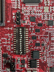
There are multiple sources as shown in Figure 2-4 such as 40 pin LP/BP, DCA1000 EVM, onboard FTDI and XDS110 that can control the Radar front-end chip in the starter kit. This is done with the help of mux scheme implemented on the MMWAVEICBOOST. Follow the switch settings as shown in Table 2-1 to avoid the conflicts. The most used configuration is the default position.

GUID-4AE2F1D9-5D34-46C8-8F68-838B58E7580E-low.gifFigure 2-4 Muxing Scheme

Table 2-1 shows the dip switch settings for multiple sources connecting to mmWave sensing device.

Table 2-1 Switch Settings
Reference Designator(Default Position) Position for STAND ALONE Mode (1)Position for DCA1000 ModePosition for 40-Pin LP/BP
GUID-658C7969-8B5B-4D6B-AF4B-5EBE93A83D21-low.gifGUID-FA5A3636-B8C6-488D-A7B0-02147297F1D5-low.gifGUID-41FE2883-566A-453A-A73E-17A44C076961-low.gif
S1.12ONONON
S1.11ONONOFF
S1.10ONONOFF
S1.9OFFOFFON
S1.8OFFOFFON
S1.7ONOFFOFF
S1.6ONOFFOFF
S1.5(2)ONONOFF
S1.4ONOFFON
S1.3ONONOFF
S1.2ONONON
S1.1OFFOFFOFF
Standalone mode means starter kit and MMWAVEICBOOST connected together.
S1.5 has RS232 connections from 40 pin/FTDI/60 pin/XDS110, ON postion routes UART to XDS110 (Application/user UART COM port).

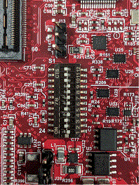
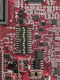
Table 2-2 shows the images of NRST, DIP switch settings, SOP lines, and power input locations on the physical board.

Table 2-2 Mux Selection Images
FrontRear
Whole Board
GUID-C2992F1D-95E9-44FA-B660-B3FDB183A844-low.png Figure 2-5 Front
GUID-BF30BD48-5898-47B2-BFA9-C42444DB694E-low.pngFigure 2-6 Rear
Zoomed IN
GUID-C98ECDD1-FA5B-46CF-BAD0-84B8EEC67499-low.pngFigure 2-7 Front