SWRU546E October 2018 – May 2022 AWR6843 , AWR6843AOP , IWR6443 , IWR6843 , IWR6843AOP
- Trademarks
- 1Getting Started
-
2MMWAVEICBOOST
- 2.1 Hardware
- 2.2 Block Diagram and Features
- 2.3 Muxing Scheme for Multiple Sources
- 2.4 Using the MMWAVEICBOOST With the Starter Kit
- 2.5 Interfacing with the DCA1000EVM
- 2.6 Power Connections
- 2.7
Connectors
- 2.7.1 20-Pin LaunchPad and Booster Pack Connectors (J5, J6)
- 2.7.2 60-Pin High Density (HD) Connector (J4 and J17)
- 2.7.3 60-Pin High Density (HD) Connector (J10)
- 2.7.4 MIPI 60-Pin Connector (J9)
- 2.7.5 TI 14-Pin JTAG Connector (J19)
- 2.7.6 CAN Connector (J1 and J2)
- 2.7.7 Ultra-Miniature Coaxial Connector (J3)
- 2.8 Jumpers, Switches and LEDs
- 3xWR6843ISK / IWR6843ISK-ODS REV C
-
4xWR6843AOPEVM Rev G
- 4.1 Hardware
- 4.2 Block Diagram
- 4.3 PCB Storage and Handling Recommendations
- 4.4 Heat Sink and Temperature
- 4.5 xWR6843AOPEVM Antenna
- 4.6 Switch Settings
- 4.7 xWR6843AOPEVM Muxing Scheme
- 4.8 Modular, DCA1000EVM and MMWAVEICBOOST Mode
- 4.9 Known Issues: Spurious Performance
- 4.10 PC Connection
- 4.11 REACH Compliance
- 4.12 Regulatory Statements with Respect to the xWR6843AOPEVM Rev G
- 5xWR6843AOPEVM Rev F
- 6IWR6843ISK / IWR6843ISK-ODS (deprecated)
- 7IWR6843AOPEVM (Deprecated)
- 8TI E2E Community
- 9Certification Related Information
- Revision History
2.7.1 20-Pin LaunchPad and Booster Pack Connectors (J5, J6)
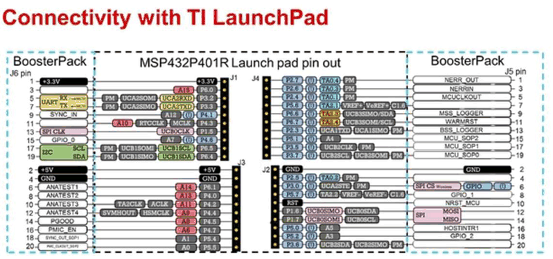
The MMWAVEICBOOST has the standard LaunchPad connectors (J5 and J6) that enable it to be directly connected to all TI MCU LaunchPad's pinout, as shown in Figure 2-17. While connecting the MMWAVEICBOOST to other LaunchPads, ensure the pin-1 orientation is correct by matching the 3V3 and 5-V signal marking on the boards. Figure 2-17 shows two 20-pin connectors.
Table 2-4 and Table 2-5 provide the connector pin information.
 Figure 2-17 TI Standard LaunchPad
Table 2-4 J6 Connector Pinout
| Pin Number | Description | Pin Number | Description |
|---|---|---|---|
| 1 | NERROUT | 2 | GND |
| 3 | NERRIN | 4 | DSS LOGGER |
| 5 | MCUCLKOUT | 6 | SPI_CS |
| 7 | NC | 8 | GPIO1 |
| 9 | MSS LOGGER (data from xWR device) (1) | 10 | nRESET |
| 11 | WARMRST | 12 | SPI_MOSI |
| 13 | BSS LOGGER | 14 | SPI_MISO |
| 15 | SOP2 | 16 | HOSTINT |
| 17 | SOP1 | 18 | GPIO2 |
| 19 | SOP0 | 20 | NC |
(1) When running the OOB demo, the MSS_Logger pin is used to send
data. This is the same pin connected to the XDS110 and displayed through the
emulator as a data COM port.
Table 2-5 J5 Connector Pinout
| Pin Number | Description | Pin Number | Description |
|---|---|---|---|
| 1 | 3V3 | 2 | 5V |
| 3 | NC | 4 | GND |
| 5 | RS232 (TX from xWR device)(1) | 6 | NC |
| 7 | RS232 (RX into xWR device)(1) | 8 | NC |
| 9 | SYNC_IN | 10 | NC |
| 11 | NC | 12 | NC |
| 13 | SPI_CLK | 14 | PGOOD (2) |
| 15 | GPIO0 | 16 | PMIC_Enable (3) |
| 17 | SCL | 18 | SYNC_OUT |
| 19 | SDA | 20 | PMIC CLKOUT |
(1) When running the OOB demo, the
RS232 TX and RX pins are used for user and configuration files. This is the same
pin connected to the XDS110 and displayed through the emulator as a
Application/User UART COM port.
(2) Indicates that all the powers are
stable in the standard LP/BP boards are stable, which enables or disables the
power of FTDI and XDS110 interfaces. A HIGH on the PGOOD signal (3.3 V)
indicates the supply is stable. The I/Os of the front-end chip are not safe to
operate by the XDS110/FTDI before this I/O supply is stable, to avoid leakage
current into the I/Os.
(3) Controls the PMIC enable for
starter kits. The MCU can use this to shut down the PMIC and xWR device during
the periods it does not use the xWR device and save power. The power up of the
PMIC takes approximately 5 ms once the enable signal is made high.