SWRU546E October   2018  – May 2022 AWR6843 , AWR6843AOP , IWR6443 , IWR6843 , IWR6843AOP


  1.   Trademarks
  2. 1Getting Started
    1. 1.1 Introduction
    2. 1.2 Key Features
      1. 1.2.1 Summary of Features
      2. 1.2.2 xWR6843ISK
      3. 1.2.3 IWR6843ISK-ODS (Overhead Detection Sensing)
      4. 1.2.4 IWR6843AOP
      5. 1.2.5 MMWAVEICBOOST
    3. 1.3 What’s Included
      1. 1.3.1 Kit Contents
        1. 1.3.1.1 xWR6843ISK
        2. 1.3.1.2 IWR6843ISK-ODS
        3. 1.3.1.3 IWR6843AOPEVM
        4. 1.3.1.4 MMWAVEICBOOST
  3. 2MMWAVEICBOOST
    1. 2.1 Hardware
    2. 2.2 Block Diagram and Features
      1. 2.2.1 Block Diagram
      2. 2.2.2 Hardware Features
    3. 2.3 Muxing Scheme for Multiple Sources
    4. 2.4 Using the MMWAVEICBOOST With the Starter Kit
      1. 2.4.1 PC Connection
      2. 2.4.2 Flashing the QSPI Flash on the Antenna Module
      3. 2.4.3 MMWAVEICBOOST and Antenna Module Connections for Modular Testing
    5. 2.5 Interfacing with the DCA1000EVM
      1. 2.5.1 mmWave Studio Interface
      2. 2.5.2 MMWAVEICBOOST and Antenna Module Configuration
      3. 2.5.3 DCA1000 EVM Connection
    6. 2.6 Power Connections
    7. 2.7 Connectors
      1. 2.7.1 20-Pin LaunchPad and Booster Pack Connectors (J5, J6)
      2. 2.7.2 60-Pin High Density (HD) Connector (J4 and J17)
      3. 2.7.3 60-Pin High Density (HD) Connector (J10)
      4. 2.7.4 MIPI 60-Pin Connector (J9)
      5. 2.7.5 TI 14-Pin JTAG Connector (J19)
      6. 2.7.6 CAN Connector (J1 and J2)
      7. 2.7.7 Ultra-Miniature Coaxial Connector (J3)
    8. 2.8 Jumpers, Switches and LEDs
      1. 2.8.1 Sense on Power (SOP) Jumpers
      2. 2.8.2 I2C Connections
        1. 2.8.2.1 Default I2C Address
        2. 2.8.2.2 43
        3. 2.8.2.3 3.3-V Rail Options
        4. 2.8.2.4 Miscellaneous Headers
        5. 2.8.2.5 Switches and LEDs
          1. 2.8.2.5.1 Switches
  4. 3xWR6843ISK / IWR6843ISK-ODS REV C
    1. 3.1  Hardware
      1. 3.1.1 xWR6843ISK EVM
      2. 3.1.2 IWR6843ISK-ODS EVM
    2. 3.2  xWR6843ISK/IWR6843ISK-ODS Block Diagram
    3. 3.3  PCB Storage and Handling Recommendations
    4. 3.4  Power Connections
      1. 3.4.1 Higher Power Applications
    5. 3.5  Interfaces
      1. 3.5.1 Switches, Buttons and Muxes
      2. 3.5.2 List of LEDs
      3. 3.5.3 CANFD
      4. 3.5.4 I2C Connections
        1. 3.5.4.1 EEPROM
        2. 3.5.4.2 Default I2C Address
    6. 3.6  xWR6843ISK Antenna
    7. 3.7  IWR6843ISK-ODS Antenna
    8. 3.8  Modular Mode
    9. 3.9  DCA1000EVM Mode
    10. 3.10 MMWAVEICBOOST Mode
  5. 4xWR6843AOPEVM Rev G
    1. 4.1  Hardware
    2. 4.2  Block Diagram
    3. 4.3  PCB Storage and Handling Recommendations
    4. 4.4  Heat Sink and Temperature
    5. 4.5  xWR6843AOPEVM Antenna
    6. 4.6  Switch Settings
    7. 4.7  xWR6843AOPEVM Muxing Scheme
      1. 4.7.1 SOP Configuration
    8. 4.8  Modular, DCA1000EVM and MMWAVEICBOOST Mode
      1. 4.8.1 Modular Mode
      2. 4.8.2 DCA1000EVM Mode
      3. 4.8.3 MMWAVEICBOOST Mode
    9. 4.9  Known Issues: Spurious Performance
    10. 4.10 PC Connection
      1. 4.10.1 Installing the Drivers
      2. 4.10.2 Flashing the Board
    11. 4.11 REACH Compliance
    12. 4.12 Regulatory Statements with Respect to the xWR6843AOPEVM Rev G
  6. 5xWR6843AOPEVM Rev F
    1. 5.1  Hardware
    2. 5.2  Block Diagram
    3. 5.3  PCB Storage and Handling Recommendations
    4. 5.4  Heat Sink and Temperature
    5. 5.5  xWR6843AOPEVM Antenna
    6. 5.6  Switch Settings
    7. 5.7  xWR6843AOPEVM Muxing Scheme
      1. 5.7.1 SOP Configuration
    8. 5.8  Modular and MMWAVEICBOOST Mode
      1. 5.8.1 Modular Mode
      2. 5.8.2 MMWAVEICBOOST Mode
    9. 5.9  PC Connection
      1. 5.9.1 Installing the Drivers
      2. 5.9.2 Flashing the Board
      3. 5.9.3 DCA1000
    10. 5.10 REACH Compliance
  7. 6IWR6843ISK / IWR6843ISK-ODS (deprecated)
    1. 6.1 Hardware
      1. 6.1.1 IWR6843ISK EVM
      2. 6.1.2 IWR6843ISK-ODS EVM
    2. 6.2 IWR6843ISK/IWR6843ISK-ODS Block Diagram
    3. 6.3 PCB Storage and Handling Recommendations
    4. 6.4 Power Connections
    5. 6.5 Miscellaneous and LEDs
      1. 6.5.1 List of LEDs
      2. 6.5.2 I2C Connections
        1. 6.5.2.1 EEPROM
        2. 6.5.2.2 Default I2C Address
    6. 6.6 IWR6843ISK Antenna
    7. 6.7 IWR6843ISK-ODS Antenna
  8. 7IWR6843AOPEVM (Deprecated)
    1. 7.1 Hardware
    2. 7.2 Block Diagram
    3. 7.3 PCB Storage and Handling Recommendations
    4. 7.4 IWR6843AOPEVM Antenna
    5. 7.5 Switch Settings
    6. 7.6 IWR6843AOPEVM Muxing Scheme
      1. 7.6.1 SOP Configuration
    7. 7.7 Modular and MMWAVEICBOOST Mode
      1. 7.7.1 Modular Mode
      2. 7.7.2 MMWAVEICBOOST Mode
    8. 7.8 PC Connection
      1. 7.8.1 Installing the Drivers
      2. 7.8.2 Flashing the Board
      3. 7.8.3 DCA1000
    9. 7.9 REACH Compliance
  9. 8TI E2E Community
  10. 9Certification Related Information
  11.   Revision History

Hardware

The xWR6843AOPEVM includes four receivers and three transmitter wide field of antennas on the package of the device. The IWR6843AOP and AWR6843AOP operate at a 4-Ghz bandwidth from 60 to 64 GHz, with a maximum output power of 10 dBm; the xWR6843AOPEVM has an antenna gain of ~5 dBi.

Note:

The xWR6843AOPEVM has been tested in the 60 - 64GHz band across the temperature range of -20°C to 60°C.

Note:

In accordance to the EN 62311 RF exposure test, a minimum separation distance of 20 centimeters should be maintained between the user and the EVM during operation.

Note:

Refer to the Thermal Design Guide for Antenna on Package mmWave Sensor application note for details of thermal dissipation options for xWR6843 AOP devices, particularly for small form factor designs such as the mission side of the EVM.

GUID-66EDD7C6-7BF9-4E23-AD81-2B8B433EAE61-low.jpgFigure 5-1 xWR6843AOPEVM Top View

When split, the following features are available:

  • 60-GHz to 64-GHz mmWave sensing for form-factor deployment and testing
  • Functional and flashing SOP Mode
  • Emulator USB port for user UART and Data COM ports
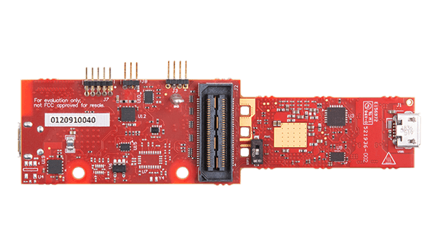
GUID-E1059DB9-2603-4F57-9EF1-6F800492D22C-low.pngFigure 5-2 xWR6843AOPEVM Bottom View
CAUTION:

There is a possibility of damage and lose of function to the mission board when it is split. When split, the board cannot be put back together and many features are lost; see the Section 5.1 section for features available on the mission board. Raw data capture, JTAG debug and other features requiring the 60 pin SAMTEC connectors are permanently lost.