SWRU613 july 2023 AWRL1432
- 1
- Description
- Get Started
- Features
- 5
- 1Evaluation Module Overview
-
2Hardware
- 2.1 XWRL1432BOOST Antenna
- 2.2 EVM Mux Block Diagram
- 2.3 Switch Settings
- 2.4 LEDs
- 2.5 Connectors
- 2.6 USB Connector
- 2.7 DCA1000 HD Connector
- 2.8 Booster Pack Connector for the LaunchPad Connectivity
- 2.9 CANFD Connector
- 2.10 LIN PHY Connection
- 2.11 I2C Connections
- 2.12 XDS110 Interface
- 2.13 Flashing the Board
- 2.14 DCA1000EVM Mode
- 2.15 PCB Storage and Handling Recommendations:
- 3Software
- 4Hardware Design Files
- 5Additional Information
- 6References
2.3 Switch Settings
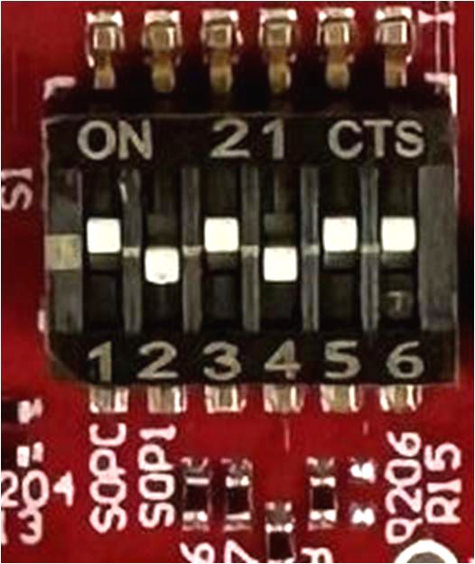
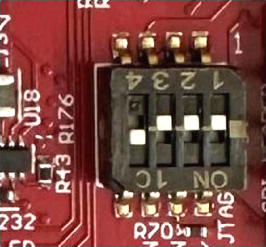
Figure 3-10 shows the part designators and positions of the switches (S1 and S4) on the XWRL1432BOOST.
 Figure 2-10 S1 Switch for Various Mode Settings
 Figure 2-11 S4 Switch for
Various Mode Settings
Figure 2-11 S4 Switch for
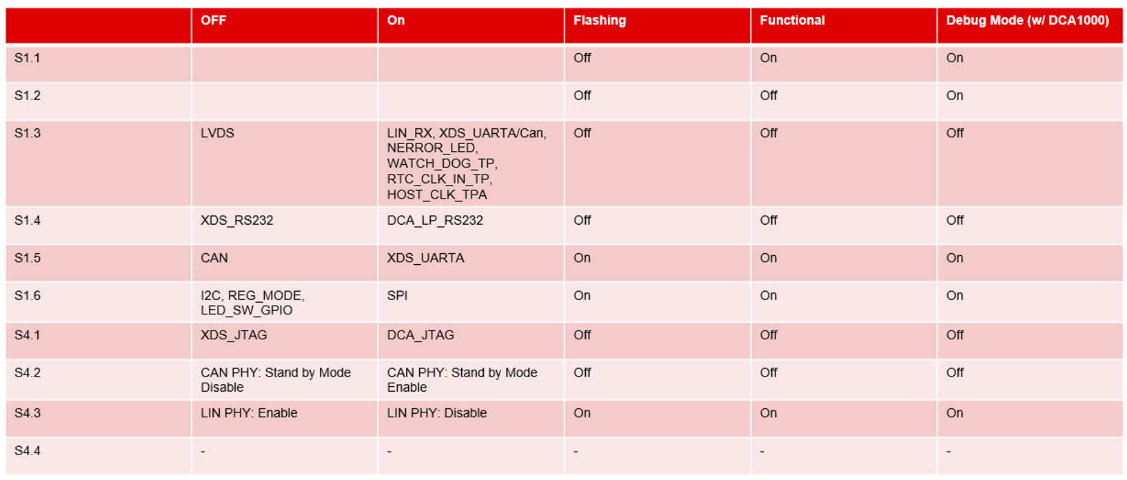
Various Mode SettingsFigure 3-12 provides the different boot mode configurations to the device. Device supports application mode, QSPI flashing mode (Device management mode), and debug modes. This mode (SOP) configuration shown below in Figure 3-12 must be exercised first. After the SOP settings nRESET need to be issued to register the SOP settings. Figure 3-12 also provides the switch position for different modes of operation supported by the device and EVM.
 Figure 2-12 SOP Switches