SWRU613 july 2023 AWRL1432
- 1
- Description
- Get Started
- Features
- 5
- 1Evaluation Module Overview
-
2Hardware
- 2.1 XWRL1432BOOST Antenna
- 2.2 EVM Mux Block Diagram
- 2.3 Switch Settings
- 2.4 LEDs
- 2.5 Connectors
- 2.6 USB Connector
- 2.7 DCA1000 HD Connector
- 2.8 Booster Pack Connector for the LaunchPad Connectivity
- 2.9 CANFD Connector
- 2.10 LIN PHY Connection
- 2.11 I2C Connections
- 2.12 XDS110 Interface
- 2.13 Flashing the Board
- 2.14 DCA1000EVM Mode
- 2.15 PCB Storage and Handling Recommendations:
- 3Software
- 4Hardware Design Files
- 5Additional Information
- 6References
2.14 DCA1000EVM Mode
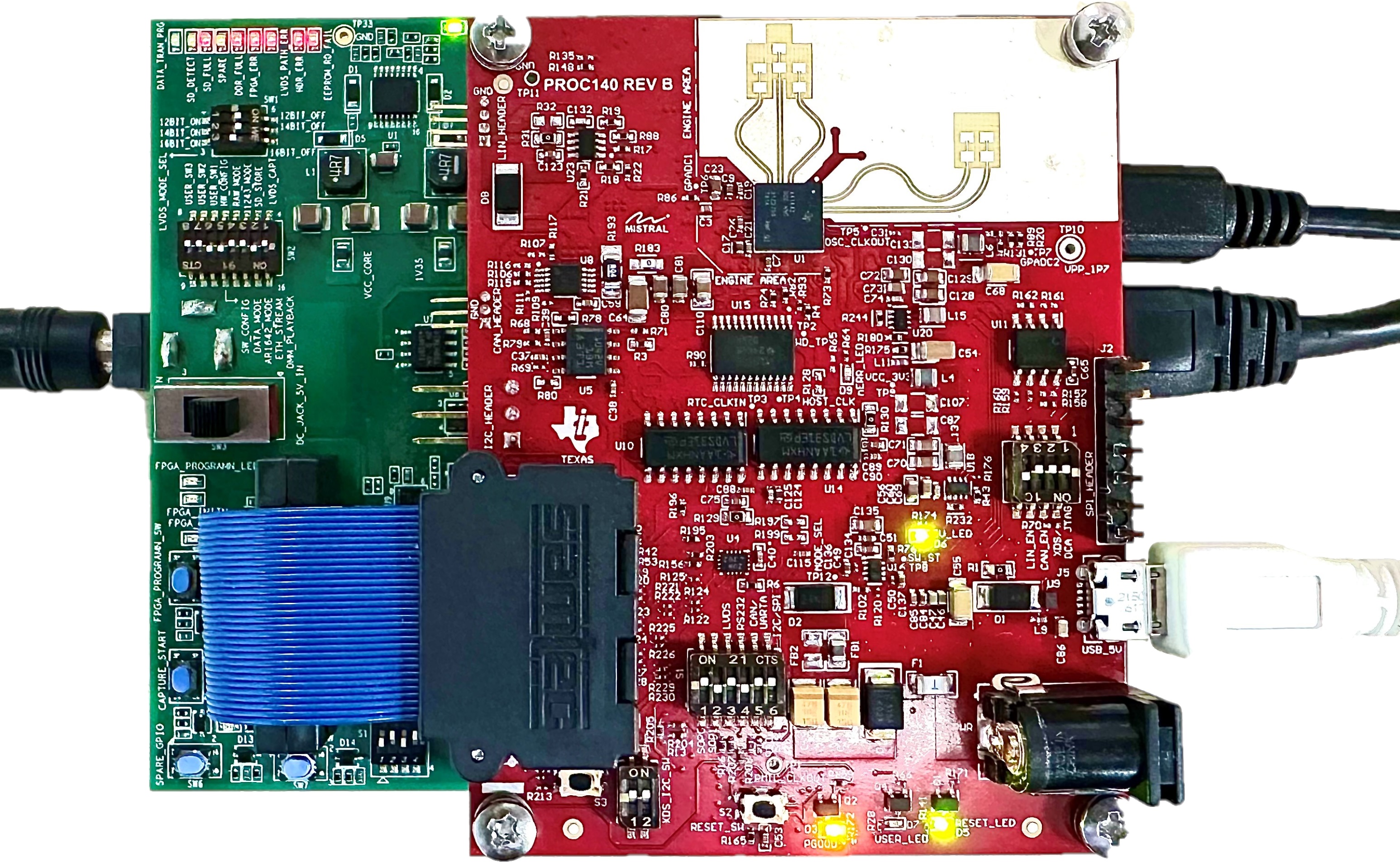
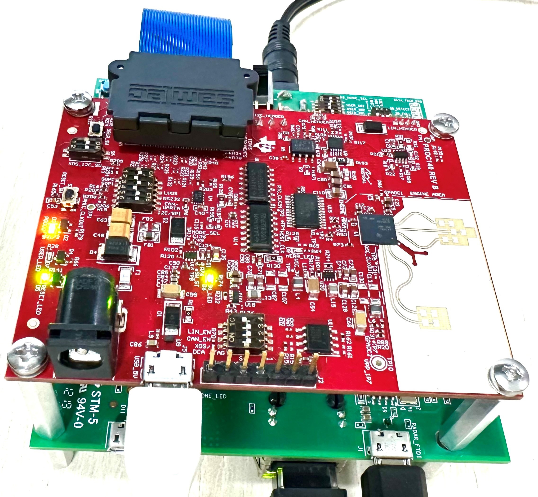
The setup for raw data capture using DCA1000EVM is shown in Figure 3-23.
 Figure 2-23 DCA1000EVM Mode (Top View)
 Figure 2-24 DCA1000EVM Mode (Side View)
Please refer to Figure 3-12 shown in the beginning of this document for the switch settings for the DCA1000 raw ADC capture card.