TIDU312A May 2014 – November 2020
- Trademarks
- 1Introduction
- 2Software Overview
- 3Procedure for Running the Incremental Builds
- 4Test Results
- 5References
- 6Revision History
1.1 PFC Stage Implementation
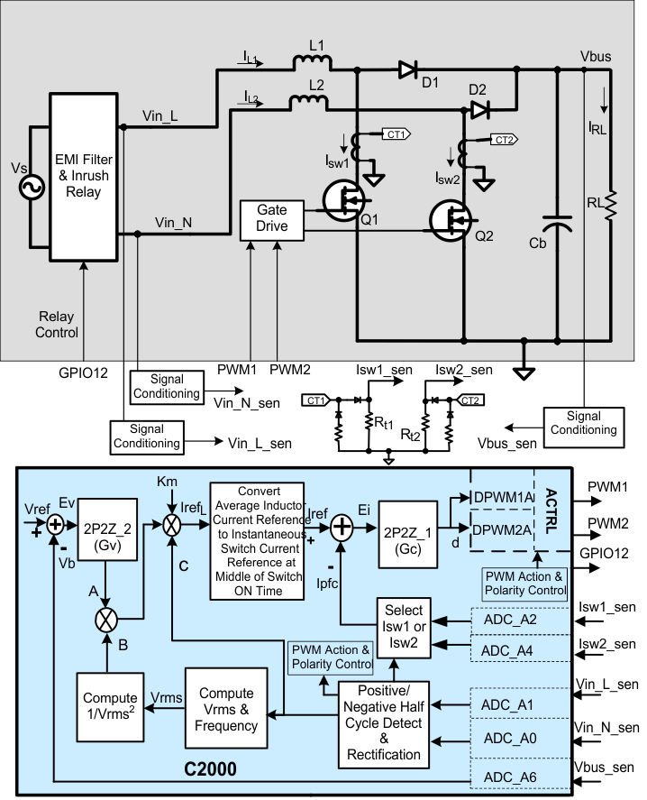
Figure 1-1 illustrates a C2000 based bridgeless PFC converter control system. The input AC voltage is applied to the PFC converter through the input EMI filter followed by an inrush control relay. The PFC stage consists of two boost converters each operating alternately in boost mode during half of the input AC line cycle.
 Figure 1-1 Bridgeless PFC Converter
Control Using C2000 Microcontroller
Figure 1-1 Bridgeless PFC Converter
Control Using C2000 MicrocontrollerDuring one half of the line cycle one converter converts the AC line voltage to the DC bus voltage, while the other converter performs the same action during the other half of the line cycle. Inductor L1, MOSFET switch Q1, current sense transformer CT1 and diode D1 together form one of the boost stages while, L2, Q2, CT2 and D2 form the other boost stage. A capacitor Cb at the boost converter output acts as an energy reservoir and provides regulated dc voltage to the PFC load denoted by RL.
Figure 1-1 indicates all the interface signals needed for full control of this bridgeless PFC converter using a C2000 microcontroller (MCU). The MCU controls the hardware using five feedback signals, two PWM outputs and one GPIO output. The signals that are sensed and fed back to the MCU include, the line and neutral voltages (Vin_L & Vin_N), the two PFC switch currents (Isw1, Isw2), and the boost output voltage (Vbus). These sensed signals are used to implement the voltage and current control loops for this BL PFC converter.
The dc bus voltage Vbus, sensed through one of the ADC channels, is compared against the reference bus voltage Vref. The resulting error signal Ev is then input the voltage loop controller Gv which regulates the bus voltage at the reference level. The voltage controller Gv has the form of a two pole two zero (2P2Z) compensator. The output of Gv, denoted by the letter A in Figure 1-1, is proportional to the amount of power transfer by the PFC converter. This output A is then multiplied by three parameters, indicated by B, C and Km in Figure 1-1, in order to form the reference current command Iref for the PFC current control loop. The signal indicated by B is the inverse of the square of the RMS input voltage which enables fast feed-forward control of the PFC system. The signal C is proportional to the rectified input voltage, which modulates the voltage controller output A such that the PFC input current has the same shape of the PFC input voltage. The parameter Km is called the multiplier gain which is used to adjust the range of Iref corresponding to the full input voltage range of the PFC converter. The output of the multiplier provides the reference signal for control of average inductor current IrefL. However, for BL PFC system the current feedback is from the PFC switches (Q1 & Q2), and not from the boost inductors (L1 & L2). This means the reference signal IrefL for average inductor current control has to be converted before it is used for PFC switch current control. In Figure 1-1 this is indicated by the conversion block between IrefL and Iref. This reference current command Iref for the PFC current control loop is then compared against the PFC switch current Ipfc sensed through two ADC channels. The resulting current error signal Ei is then input the current loop controller Gc which generates the PFC duty ratio command d such that the PFC switch current tracks the reference current Iref.
In addition to implementing the voltage and current loop controllers, C2000 MCU also uses the sensed line and neutral voltage signals to determine the polarity of the input voltage (+ve & –ve half cycle) and to calculate the rectified input voltage, the RMS input voltage and the input line frequency. Based on the polarity of the input voltage the C2000 controller selects the appropriate PFC switch current (Isw1 or Isw2) to be used as PFC current feedback Ipfc. The polarity information is also used to set the appropriate PFC switch (Q1 & Q2) to either in PWM mode (boost PFC) or in forced ON mode. All these time critical functions are implemented in a fast sampling loop enabled by the C2000 Microcontroller high speed CPU, interrupts, on chip 12-bit ADC module and high frequency PWM modules. A detailed description of the software algorithm is provided in the following chapters.