TIDU312A May 2014 – November 2020
- Trademarks
- 1Introduction
- 2Software Overview
- 3Procedure for Running the Incremental Builds
- 4Test Results
- 5References
- 6Revision History
3.1.4.4.2 Step 1.6: Run the Code for Build 1
- Run the code by using the <F8> key, or using the Run button on the toolbar, or using Target -> Run on the menu bar.
- In the watch view, add the variable DutyA and set it to 0.1 (=1677721 in Q24). This variable sets the duty cycle for the PFC converter.
- Apply an appropriate resistive load to the PFC system at the DC output (10~100W).
- Apply AC Power to the board. Measure and verify the DC bus voltage corresponding to applied input voltage and the duty ratio.
- Use DutyA to slowly change the
duty from the watch window. The boost converter output voltage should change
accordingly. Note:
Observe the output voltage carefully, this should not be allowed to exceed the maximum voltage rating of the board.
- Add the other variables such as, Vbus, VL_fb, VN_fb and verify the different ADC results in the watch view. For AC voltage input the sensed line and neutral voltage(VL_fb, VN_fb) will vary continuously in the watch window. Therefore, to verify the ADC readings and the line and neutral voltage sense circuits, the user may apply DC input voltage (20~200V) instead of AC (as stated in step 20 above). In that case the PFC stage will temporarily operate in a pure dc-dc boost mode.
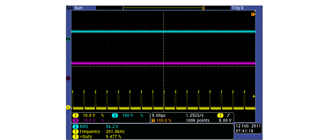
- The following oscilloscope
captures show two PWM outputs (Ch1 & Ch3) and the DC input voltage (Ch2)
when the output DC bus load is 8K ohm and the set duty ratio is about 10%. Since
the input voltage in this case is always positive (+50V in this case) PWM1A will
be in PWM mode (Ch1) and PWM2A will be in forced ON mode (Ch3). The PWM
frequency is also measured to be 200kHz.
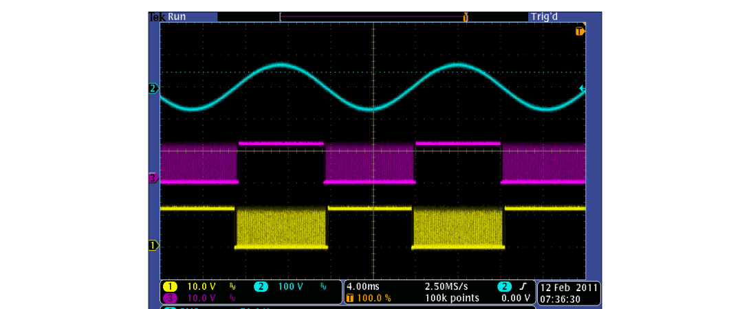
- The following oscilloscope
captures show two PWM outputs (Ch1 & Ch3) and the AC input voltage (Ch2) of
about 50V when the output DC bus load is 8K ohm and the set duty ratio is about
10%. With the AC input voltage PWM1A and PWM2A alternately switch between PWM
mode and forced ON mode.
- Try different duty cycle values and observe the corresponding ADC results. Increase duty cycle value in small steps. Always observe the output voltage carefully, this should not be allowed to exceed the capabilities of the board. Different waveforms, like the PWM gate drive signals, input voltage and current and output voltage may also be probed and verified using an oscilloscope. Appropriate safety measures must be taken while probing these high voltage signals.
- Fully halting the MCU when in real-time mode is a two-step process. With the AC input turned off wait until the DC bus capacitor is fully discharged. First, halt the processor by using the Halt button on the toolbar, or by using Target -> Halt. Then take the MCU out of real-time mode. Finally reset the MCU.
- You may choose to leave Code Composer Studio running for the next exercise or optionally close CCS.
- End of Exercise