TIDUD61E October 2020 – April 2021
- Description
- Resources
- Features
- Applications
- 5
- 1System Description
- 2System Overview
-
3Hardware, Software, Testing Requirements, and Test Results
- 3.1
Required Hardware and Software
- 3.1.1 Hardware
- 3.1.2
Software
- 3.1.2.1 Opening Project Inside CCS
- 3.1.2.2 Project Structure
- 3.1.2.3 Using CLA on C2000 MCU to Alleviate CPU Burden
- 3.1.2.4 CPU and CLA Utilization and Memory Allocation
- 3.1.2.5
Running the Project
- 3.1.2.5.1 Lab 1: Open Loop, DC (PFC Mode)
- 3.1.2.5.2 Lab 2: Closed Current Loop DC (PFC)
- 3.1.2.5.3 Lab 3: Closed Current Loop, AC (PFC)
- 3.1.2.5.4 Lab 4: Closed Voltage and Current Loop (PFC)
- 3.1.2.5.5 Lab 5: Open loop, DC (Inverter)
- 3.1.2.5.6 Lab 6: Open loop, AC (Inverter)
- 3.1.2.5.7 Lab 7: Closed Current Loop, DC (Inverter with resistive load)
- 3.1.2.5.8 Lab 8: Closed Current Loop, AC (Inverter with resistive load)
- 3.1.2.5.9 Lab 9: Closed Current Loop (Grid Connected Inverter)
- 3.1.2.6 Running Code on CLA
- 3.1.2.7
Advanced Options
- 3.1.2.7.1 Input Cap Compensation for PF Improvement Under Light Load
- 3.1.2.7.2 83
- 3.1.2.7.3 Adaptive Dead Time for Efficiency Improvements
- 3.1.2.7.4 Phase Shedding for Efficiency Improvements
- 3.1.2.7.5 Non-Linear Voltage Loop for Transient Reduction
- 3.1.2.7.6 Software Phase Locked Loop Methods: SOGI - FLL
- 3.2 Testing and Results
- 3.1
Required Hardware and Software
- 4Design Files
- 5Software Files
- 6Related Documentation
- 7About the Author
- 8Revision History
3.1.2.2 Project Structure
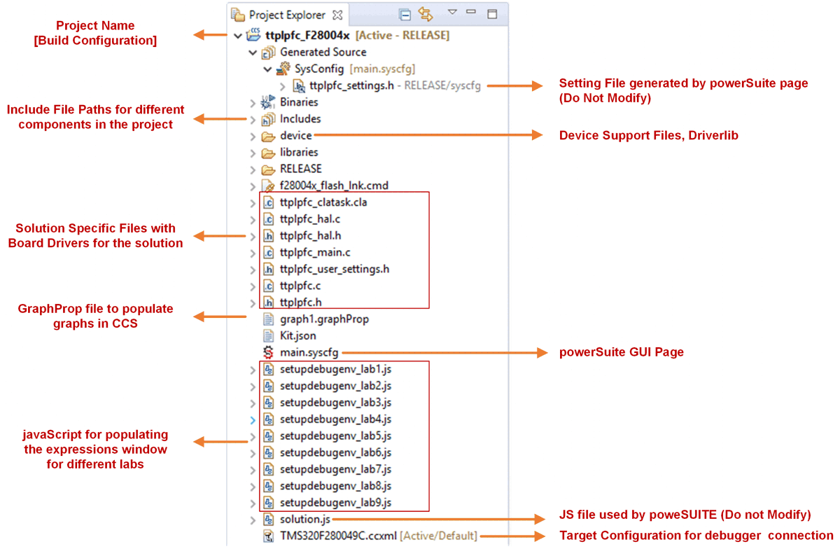
Once the project is imported, the project explorer appears inside CCS as shown in Figure 3-4.
 Figure 3-4 Project Explorer View of Solution Project
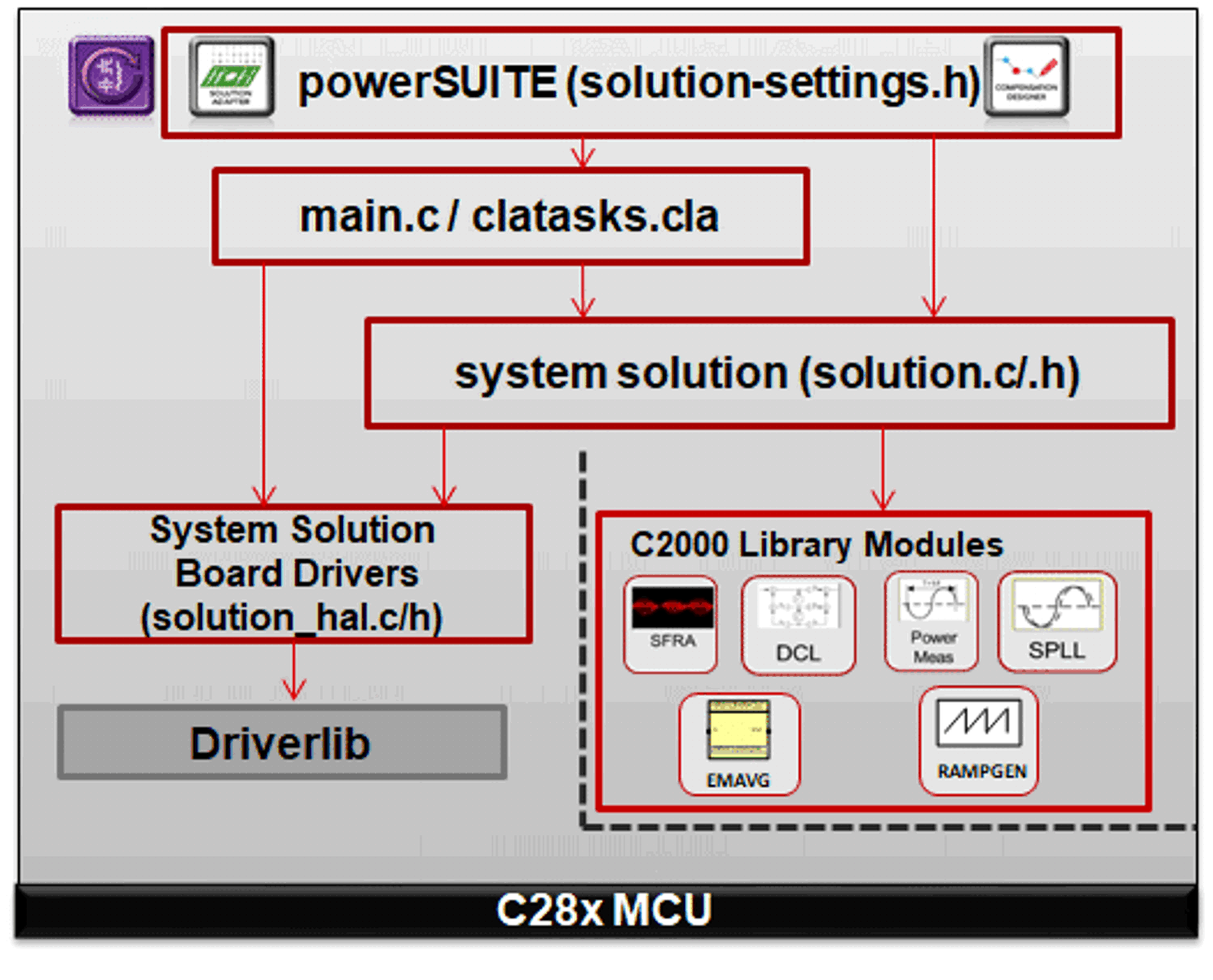
The general structure of the project is shown in Figure 3-5.
 Figure 3-5 Project Structure
Overview
Figure 3-5 Project Structure
OverviewFigure 3-5 shows the project for F28004x; however, if a different device is chosen from the powerSUITE page, the structure is similar.
Solution specific and device independent files are <solution>.c/h. This file consist of the main.c file of the project and is responsible for the control structure of the solution.
For this design <solution> is ttplpfc.
Board-specific and device-specific files are <solution>_hal.c/h. This file consists of device specific drivers to run the solution.
The powerSUITE page can be opened by clicking on the main.syscfg file, listed under the project explorer. The powerSUITE page generates the <solution>_settings.h file. This file is the only file used in the compile of the project that is generated by the powerSUITE page. The user must not modify this file manually as the changes are overwritten by powerSUITE every time the project is saved. User can modify several settings in <solution>_user_settings.h file.
The Kit.json and solution.js files are used internally by the powerSUITE and must also not be modified by the user. Any changes to these files results in project not functioning properly.
The setupdebugenv_build.js are provided to autopoulate the watch window variables for different builds
The *.graphProp files is provided to auto populate settings for the data logger graph
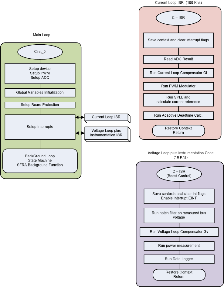
The project consists of an interrupt service routine, which is called every PWM cycle, and a current controller is run inside this ISR. In addition to this, there is a slower ISR of approximately 10 kHz that is called for running the voltage loop and the instrumentation ISR. A few background tasks (A0-A4 and B0-B4) are called in a polling fashion and can be used to run slow tasks for which absolute timing accuracy is not required, such as SFRA background and so on.
Figure 3-6 shows the software flow diagram of the firmware
 Figure 3-6 Project Structure Image
To simplify the system bring up and design the software of this reference design is organized in nine labs. The lab from 1 to 4 are designed to validate PFC operation and the lab from 5 to 9 are designed to validate the inverter operation.
- PFC Operation
- Lab 1: Open Loop (DC input)
- Lab 2: Closed Current Loop (DC input)
- Lab 3: Closed Current Loop (AC input)
- Lab 4: Closed Voltage and Current Loop (AC input)
- Inverter Operation
- Lab 5: Open Loop (DC output)
- Lab 6: Open Loop (AC output)
- Lab 7: Closed Current Loop (DC output, Resistive load)
- Lab 8: Closed Current Loop (AC output, Resistive load )
- Lab 9: Closed Current Loop (AC output , Gried-tied condition)
These labs are detailed in Section 3.1.2.5. If using the reference design hardware, make sure the hardware setup is completed as outlined in Section 3.1.1.