TIDUD61E October   2020  – April 2021


  1.   Description
  2.   Resources
  3.   Features
  4.   Applications
  5.   5
  6. 1System Description
    1. 1.1 Key System Specifications
  7. 2System Overview
    1. 2.1 Block Diagram
    2. 2.2 Design Considerations
      1. 2.2.1 Input AC Voltage Sensing
      2. 2.2.2 Bus Voltage Sensing
      3. 2.2.3 AC Current Sensing
      4. 2.2.4 Sense Filter
      5. 2.2.5 Protection (CMPSS)
    3. 2.3 Highlighted Products
      1. 2.3.1 C2000™ MCU F28004x
      2. 2.3.2 LMG3410R070
      3. 2.3.3 UCC27714
    4. 2.4 System Design Theory
      1. 2.4.1 PWM
      2. 2.4.2 Current Loop Model (PFC and Inverter mode)
      3. 2.4.3 DC Bus Regulation Loop (for PFC mode only)
      4. 2.4.4 Soft Start Around Zero Crossing for Eliminate or Reduce Current Spike
      5. 2.4.5 AC Drop Test
  8. 3Hardware, Software, Testing Requirements, and Test Results
    1. 3.1 Required Hardware and Software
      1. 3.1.1 Hardware
        1. 3.1.1.1 Base Board Settings
        2. 3.1.1.2 Control Card Settings
      2. 3.1.2 Software
        1. 3.1.2.1 Opening Project Inside CCS
        2. 3.1.2.2 Project Structure
        3. 3.1.2.3 Using CLA on C2000 MCU to Alleviate CPU Burden
        4. 3.1.2.4 CPU and CLA Utilization and Memory Allocation
        5. 3.1.2.5 Running the Project
          1. 3.1.2.5.1 Lab 1: Open Loop, DC (PFC Mode)
            1. 3.1.2.5.1.1 Setting Software Options for LAB 1
            2. 3.1.2.5.1.2 Building and Loading Project
            3. 3.1.2.5.1.3 Setup Debug Environment Windows
            4. 3.1.2.5.1.4 Using Real-Time Emulation
            5. 3.1.2.5.1.5 Running Code
          2. 3.1.2.5.2 Lab 2: Closed Current Loop DC (PFC)
            1. 3.1.2.5.2.1 Setting Software Options for Lab 2
            2. 3.1.2.5.2.2 Designing Current Loop Compensator
            3. 3.1.2.5.2.3 Building and Loading Project and Setting up Debug
            4. 3.1.2.5.2.4 Running Code
          3. 3.1.2.5.3 Lab 3: Closed Current Loop, AC (PFC)
            1. 3.1.2.5.3.1 Setting Software Options for Lab 3
            2. 3.1.2.5.3.2 Building and Loading Project and Setting up Debug
            3. 3.1.2.5.3.3 Running Code
          4. 3.1.2.5.4 Lab 4: Closed Voltage and Current Loop (PFC)
            1. 3.1.2.5.4.1 Setting Software Options for Lab 4
            2. 3.1.2.5.4.2 Designing Voltage Loop Compensator
            3. 3.1.2.5.4.3 Building and Loading Project and Setting up Debug
            4. 3.1.2.5.4.4 Running Code
          5. 3.1.2.5.5 Lab 5: Open loop, DC (Inverter)
            1. 3.1.2.5.5.1 Setting Software Options for Lab 5
            2. 3.1.2.5.5.2 Building and Loading Project
            3. 3.1.2.5.5.3 Setup Debug Environment Windows
            4. 3.1.2.5.5.4 Running Code
          6. 3.1.2.5.6 Lab 6: Open loop, AC (Inverter)
            1. 3.1.2.5.6.1 Setting Software Options for Lab 6
            2. 3.1.2.5.6.2 Building and Loading Project and Setting up Debug
            3. 3.1.2.5.6.3 Running Code
          7. 3.1.2.5.7 Lab 7: Closed Current Loop, DC (Inverter with resistive load)
            1. 3.1.2.5.7.1 Setting Software Options for Lab 7
            2. 3.1.2.5.7.2 Designing Current Loop Compensator
            3. 3.1.2.5.7.3 Building and Loading Project and Setting up Debug
            4. 3.1.2.5.7.4 Running Code
          8. 3.1.2.5.8 Lab 8: Closed Current Loop, AC (Inverter with resistive load)
            1. 3.1.2.5.8.1 Setting Software Options for Lab 8
            2. 3.1.2.5.8.2 Building and Loading Project and Setting up Debug
            3. 3.1.2.5.8.3 Running Code
          9. 3.1.2.5.9 Lab 9: Closed Current Loop (Grid Connected Inverter)
            1. 3.1.2.5.9.1 Setting Software Options for Lab 9
            2. 3.1.2.5.9.2 Building and Loading Project and Setting up Debug
            3. 3.1.2.5.9.3 Running Code: Emulated Grid-tied Condition (Verification purpose only)
            4. 3.1.2.5.9.4 Running Code: Grid-tied Condition
        6. 3.1.2.6 Running Code on CLA
        7. 3.1.2.7 Advanced Options
          1. 3.1.2.7.1 Input Cap Compensation for PF Improvement Under Light Load
          2. 3.1.2.7.2 83
          3. 3.1.2.7.3 Adaptive Dead Time for Efficiency Improvements
          4. 3.1.2.7.4 Phase Shedding for Efficiency Improvements
          5. 3.1.2.7.5 Non-Linear Voltage Loop for Transient Reduction
          6. 3.1.2.7.6 Software Phase Locked Loop Methods: SOGI - FLL
    2. 3.2 Testing and Results
      1. 3.2.1 Test Results at Input 120 Vrms, 60 Hz, Output 380-V DC
        1. 3.2.1.1 Startup
        2. 3.2.1.2 Steady State Condition
        3. 3.2.1.3 Transient Test With Step Load Change
          1. 3.2.1.3.1 0% to 50% Load Step Change
          2. 3.2.1.3.2 50% to 100% Load Step Change
          3. 3.2.1.3.3 100% to 50% Load Step Change
          4. 3.2.1.3.4 50% to 100% Load Step Change
      2. 3.2.2 Test Results at Input 230 Vrms, 50 Hz, Output 380 V DC
        1. 3.2.2.1 Startup
        2. 3.2.2.2 Steady State Condition
        3. 3.2.2.3 Transient Test With Step Load Change
          1. 3.2.2.3.1 33% to 100% Load Step Change
          2. 3.2.2.3.2 100% to 33% Load Step Change
      3. 3.2.3 Test Results Graphs
  9. 4Design Files
    1. 4.1 Schematics
    2. 4.2 Bill of Materials
    3. 4.3 PCB Layout Recommendations
      1. 4.3.1 Layout Prints
    4. 4.4 Altium Project
    5. 4.5 Gerber Files
    6. 4.6 Assembly Drawings
  10. 5Software Files
  11. 6Related Documentation
    1. 6.1 Trademarks
  12. 7About the Author
  13. 8Revision History

Key System Specifications

Table 1-1 describes the bidirectional interleaved CCM TTPL PFC reference design power specifications.

Table 1-1 Key System Specifications
PARAMETERSPECIFICATION
PFC modeInverter mode (grid-tied)
Input voltageAC 120 Vrms VL-N, 60 Hz
or
AC 230 Vrms VL-N , 50 Hz
380-V DC bus Nominal
Input current16-A RMS maximum10-A maximum
Output voltage380-V DC bus NominalAC 120 Vrms VL-N, 60 Hz
or
AC 230 Vrms VL-N , 50 Hz
Output current10-A maximum16-A RMS maximum
Power rating1.65 KW at single phase 120 Vrms
or
3.3 KW at single phase 230 Vrms
Current THD<2% at 120-Vrms L-N rated load
EfficiencyPeak 98.7% at 230-Vrms input, peak >97.7% at 120-Vrms inputPeak 98.3% at 230-Vrms output, peak >97.3% at 120-Vrms output
Primary filter inductor478 µH
Output capacitance880 µF
PWM switching frequency100 kHz
GUID-A0A6C802-7660-4661-B623-AAF67957840F-low.gif
WARNING:

TI intends this reference design to be operated in a lab environment only and does not consider it to be a finished product for general consumer use.

TI Intends this reference design to be used only by qualified engineers and technicians familiar with risks associated with handling high-voltage electrical and mechanical components, systems, and subsystems.

There are accessible high voltages present on the board. The board operates at voltages and currents that may cause shock, fire, or injury if not properly handled or applied. Use the equipment with necessary caution and appropriate safeguards to avoid injuring yourself or damaging property.

GUID-A0A6C802-7660-4661-B623-AAF67957840F-low.gif
GUID-57554921-3B41-4446-A7E0-AA652ADC7269-low.gif
GUID-169ED2B4-A729-4053-A8F2-BDD153E8E5F2-low.gif
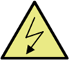
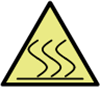
CAUTION:

Do not leave the design powered when unattended.

High voltage! There are accessible high voltages present on the board. Electric shock is possible. The board operates at voltages and currents that may cause shock, fire, or injury if not properly handled. Use the equipment with necessary caution and appropriate safeguards to avoid injuring yourself or damaging property. For safety, use of isolated test equipment with over-voltage and over-current protection is highly recommended.

TI considers it the user's responsibility to confirm that the voltages and isolation requirements are identified and understood before energizing the board or simulation. When energized, do not touch the design or components connected to the design.

Hot surface! Contact may cause burns. Do not touch!

Some components may reach high temperatures >55°C when the board is powered on. The user must not touch the board at any point during operation or immediately after operating, as high temperatures may be present.