TIDUD61E October   2020  – April 2021


  1.   Description
  2.   Resources
  3.   Features
  4.   Applications
  5.   5
  6. 1System Description
    1. 1.1 Key System Specifications
  7. 2System Overview
    1. 2.1 Block Diagram
    2. 2.2 Design Considerations
      1. 2.2.1 Input AC Voltage Sensing
      2. 2.2.2 Bus Voltage Sensing
      3. 2.2.3 AC Current Sensing
      4. 2.2.4 Sense Filter
      5. 2.2.5 Protection (CMPSS)
    3. 2.3 Highlighted Products
      1. 2.3.1 C2000™ MCU F28004x
      2. 2.3.2 LMG3410R070
      3. 2.3.3 UCC27714
    4. 2.4 System Design Theory
      1. 2.4.1 PWM
      2. 2.4.2 Current Loop Model (PFC and Inverter mode)
      3. 2.4.3 DC Bus Regulation Loop (for PFC mode only)
      4. 2.4.4 Soft Start Around Zero Crossing for Eliminate or Reduce Current Spike
      5. 2.4.5 AC Drop Test
  8. 3Hardware, Software, Testing Requirements, and Test Results
    1. 3.1 Required Hardware and Software
      1. 3.1.1 Hardware
        1. 3.1.1.1 Base Board Settings
        2. 3.1.1.2 Control Card Settings
      2. 3.1.2 Software
        1. 3.1.2.1 Opening Project Inside CCS
        2. 3.1.2.2 Project Structure
        3. 3.1.2.3 Using CLA on C2000 MCU to Alleviate CPU Burden
        4. 3.1.2.4 CPU and CLA Utilization and Memory Allocation
        5. 3.1.2.5 Running the Project
          1. 3.1.2.5.1 Lab 1: Open Loop, DC (PFC Mode)
            1. 3.1.2.5.1.1 Setting Software Options for LAB 1
            2. 3.1.2.5.1.2 Building and Loading Project
            3. 3.1.2.5.1.3 Setup Debug Environment Windows
            4. 3.1.2.5.1.4 Using Real-Time Emulation
            5. 3.1.2.5.1.5 Running Code
          2. 3.1.2.5.2 Lab 2: Closed Current Loop DC (PFC)
            1. 3.1.2.5.2.1 Setting Software Options for Lab 2
            2. 3.1.2.5.2.2 Designing Current Loop Compensator
            3. 3.1.2.5.2.3 Building and Loading Project and Setting up Debug
            4. 3.1.2.5.2.4 Running Code
          3. 3.1.2.5.3 Lab 3: Closed Current Loop, AC (PFC)
            1. 3.1.2.5.3.1 Setting Software Options for Lab 3
            2. 3.1.2.5.3.2 Building and Loading Project and Setting up Debug
            3. 3.1.2.5.3.3 Running Code
          4. 3.1.2.5.4 Lab 4: Closed Voltage and Current Loop (PFC)
            1. 3.1.2.5.4.1 Setting Software Options for Lab 4
            2. 3.1.2.5.4.2 Designing Voltage Loop Compensator
            3. 3.1.2.5.4.3 Building and Loading Project and Setting up Debug
            4. 3.1.2.5.4.4 Running Code
          5. 3.1.2.5.5 Lab 5: Open loop, DC (Inverter)
            1. 3.1.2.5.5.1 Setting Software Options for Lab 5
            2. 3.1.2.5.5.2 Building and Loading Project
            3. 3.1.2.5.5.3 Setup Debug Environment Windows
            4. 3.1.2.5.5.4 Running Code
          6. 3.1.2.5.6 Lab 6: Open loop, AC (Inverter)
            1. 3.1.2.5.6.1 Setting Software Options for Lab 6
            2. 3.1.2.5.6.2 Building and Loading Project and Setting up Debug
            3. 3.1.2.5.6.3 Running Code
          7. 3.1.2.5.7 Lab 7: Closed Current Loop, DC (Inverter with resistive load)
            1. 3.1.2.5.7.1 Setting Software Options for Lab 7
            2. 3.1.2.5.7.2 Designing Current Loop Compensator
            3. 3.1.2.5.7.3 Building and Loading Project and Setting up Debug
            4. 3.1.2.5.7.4 Running Code
          8. 3.1.2.5.8 Lab 8: Closed Current Loop, AC (Inverter with resistive load)
            1. 3.1.2.5.8.1 Setting Software Options for Lab 8
            2. 3.1.2.5.8.2 Building and Loading Project and Setting up Debug
            3. 3.1.2.5.8.3 Running Code
          9. 3.1.2.5.9 Lab 9: Closed Current Loop (Grid Connected Inverter)
            1. 3.1.2.5.9.1 Setting Software Options for Lab 9
            2. 3.1.2.5.9.2 Building and Loading Project and Setting up Debug
            3. 3.1.2.5.9.3 Running Code: Emulated Grid-tied Condition (Verification purpose only)
            4. 3.1.2.5.9.4 Running Code: Grid-tied Condition
        6. 3.1.2.6 Running Code on CLA
        7. 3.1.2.7 Advanced Options
          1. 3.1.2.7.1 Input Cap Compensation for PF Improvement Under Light Load
          2. 3.1.2.7.2 83
          3. 3.1.2.7.3 Adaptive Dead Time for Efficiency Improvements
          4. 3.1.2.7.4 Phase Shedding for Efficiency Improvements
          5. 3.1.2.7.5 Non-Linear Voltage Loop for Transient Reduction
          6. 3.1.2.7.6 Software Phase Locked Loop Methods: SOGI - FLL
    2. 3.2 Testing and Results
      1. 3.2.1 Test Results at Input 120 Vrms, 60 Hz, Output 380-V DC
        1. 3.2.1.1 Startup
        2. 3.2.1.2 Steady State Condition
        3. 3.2.1.3 Transient Test With Step Load Change
          1. 3.2.1.3.1 0% to 50% Load Step Change
          2. 3.2.1.3.2 50% to 100% Load Step Change
          3. 3.2.1.3.3 100% to 50% Load Step Change
          4. 3.2.1.3.4 50% to 100% Load Step Change
      2. 3.2.2 Test Results at Input 230 Vrms, 50 Hz, Output 380 V DC
        1. 3.2.2.1 Startup
        2. 3.2.2.2 Steady State Condition
        3. 3.2.2.3 Transient Test With Step Load Change
          1. 3.2.2.3.1 33% to 100% Load Step Change
          2. 3.2.2.3.2 100% to 33% Load Step Change
      3. 3.2.3 Test Results Graphs
  9. 4Design Files
    1. 4.1 Schematics
    2. 4.2 Bill of Materials
    3. 4.3 PCB Layout Recommendations
      1. 4.3.1 Layout Prints
    4. 4.4 Altium Project
    5. 4.5 Gerber Files
    6. 4.6 Assembly Drawings
  10. 5Software Files
  11. 6Related Documentation
    1. 6.1 Trademarks
  12. 7About the Author
  13. 8Revision History

Protection (CMPSS)

Most power electronics converters require protection from overcurrent event. For this design multiple comparators are required, and references for the trip must be generated, as shown in Figure 2-6.

GUID-A2981230-72B7-4680-94B1-61CEE2F98311-low.gifFigure 2-6 Trip Generation for PWM Using Comparators and Reference Generators

All this circuitry is avoided when using C2000 MCUs, such as TMS320F28377D, which have on-chip windowed comparator as part of the CMPSS that are internally connected to the PWM module that can enable fast tripping of the PWM. An on-chip windowed comparator saves board space and cost in the end application as extra components can be avoided using on-chip resources, as shown in Figure 2-7.
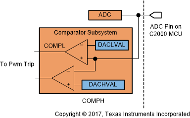
GUID-6E8CD1D6-5894-4038-9091-037062B7F01E-low.gifFigure 2-7 CMPSS Used for Overcurrent Protection