TIDUD61E October 2020 – April 2021
- Description
- Resources
- Features
- Applications
- 5
- 1System Description
- 2System Overview
-
3Hardware, Software, Testing Requirements, and Test Results
- 3.1
Required Hardware and Software
- 3.1.1 Hardware
- 3.1.2
Software
- 3.1.2.1 Opening Project Inside CCS
- 3.1.2.2 Project Structure
- 3.1.2.3 Using CLA on C2000 MCU to Alleviate CPU Burden
- 3.1.2.4 CPU and CLA Utilization and Memory Allocation
- 3.1.2.5
Running the Project
- 3.1.2.5.1 Lab 1: Open Loop, DC (PFC Mode)
- 3.1.2.5.2 Lab 2: Closed Current Loop DC (PFC)
- 3.1.2.5.3 Lab 3: Closed Current Loop, AC (PFC)
- 3.1.2.5.4 Lab 4: Closed Voltage and Current Loop (PFC)
- 3.1.2.5.5 Lab 5: Open loop, DC (Inverter)
- 3.1.2.5.6 Lab 6: Open loop, AC (Inverter)
- 3.1.2.5.7 Lab 7: Closed Current Loop, DC (Inverter with resistive load)
- 3.1.2.5.8 Lab 8: Closed Current Loop, AC (Inverter with resistive load)
- 3.1.2.5.9 Lab 9: Closed Current Loop (Grid Connected Inverter)
- 3.1.2.6 Running Code on CLA
- 3.1.2.7
Advanced Options
- 3.1.2.7.1 Input Cap Compensation for PF Improvement Under Light Load
- 3.1.2.7.2 83
- 3.1.2.7.3 Adaptive Dead Time for Efficiency Improvements
- 3.1.2.7.4 Phase Shedding for Efficiency Improvements
- 3.1.2.7.5 Non-Linear Voltage Loop for Transient Reduction
- 3.1.2.7.6 Software Phase Locked Loop Methods: SOGI - FLL
- 3.2 Testing and Results
- 3.1
Required Hardware and Software
- 4Design Files
- 5Software Files
- 6Related Documentation
- 7About the Author
- 8Revision History
3.1.2.7.4 Phase Shedding for Efficiency Improvements
Phase shedding can be an effective technique to improve efficiency in interleaved application by optimizing for the conduction and the switching losses. In this design there are three phases, so three different configurations are possible as shown in Figure 3-50.
 Figure 3-50 Phase Shedding Options on TTPL PFC
In each of these modes the phase shift between each of them must be adjusted. When in two-phase mode, a 180° phase shift is desired between the PWMs, and when in three-phase mode, a 120° of phase shift is desired.
The decision to do phase shedding can be made on different parameters, such as the RMS current, power, the peak inductor current, and so on. When using RMS current the change of phases can be significantly delayed. Figure 3-51 shows phase shedding when the decision is based on RMS current. Code takes multiple AC cycles before the phases are added .
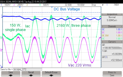 Figure 3-51 Waveform When Decision to Add Phases is Based on RMS Calculation
This delay may not be acceptable for many application. Thus, the voltage controller output is chosen as the decision point to drop or add phases. A state machine is constructed as shown in Figure 3-52, with some hysteresis built around the phase shedding points.
 Figure 3-52 State Machine for Phase Shedding Control
Bringing a phase in and out can cause in-advertent pulses to be generated. Hence the implementation to drop and add phase is done through the GPIO and PWM peripheral switch using the GPIO pin Mux registers. All PWM capable pins are configured and GPIO outputs and driven low. Now based on how many phases must be applied the GPIO pin mux is changed accordingly. It is safe to enable and disable the phases using the GPIO pin mux switch at any point in the AC cycle as the registers in the PWM are shadowed. Figure 3-53 shows details of the implementation of phase shedding on the C2000 MCU.
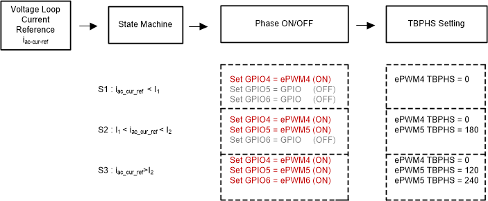 Figure 3-53 Implementation of Phase Shedding on TTPL PFC Using C2000™ MCU
The phase shedding can be set in the powerSuite page by selecting enable under the Phase shedding option. The points at which phases are brought in and out are set by changing the PHASE_SHEDDING_1PH_2PH_TRANSITION_CURRENT and PHASE_SHEDDING_2PH_3PH_TRANSITION_CURRENT define, which correspond to I1 and I2 as shown in Figure 3-53. Recompile the code, load the code, and repeat the steps as outlined in Section 3.1.2.5.4 to test this feature. With this feature implemented, under transients the phases are dropped and added quickly.
Figure 3-54 and Figure 3-55 show the transient at 110 Vrms of 1.3 KW to 150 W and vice versa. The phases are added back quickly and dropped quickly under transients as the decision is based on the voltage loop generated current reference.
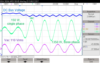 Figure 3-54 Phase Added Quickly Under Transient at 120 Vrms, 60 Hz
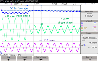 Figure 3-55 Phase Shed Quickly Under Transient at 120 Vrms, 60 Hz
Similarly at high line, a transient greater than 2 KW is applied, and the phase goes from single to three phase almost instantly. Figure 3-56 and Figure 3-56 show the test waveform at high line under transient of 2.16 KW to 150 W and vice versa.
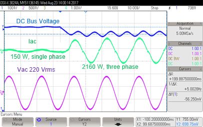 Figure 3-56 Phase Added Quickly Under Transient at 230 Vrms, 50 Hz
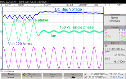 Figure 3-57 Phase Shed Quickly Under Transient at 230 Vrms, 50 Hz
Figure 3-58 shows the efficiency improvement at 230 Vrms with phase shedding
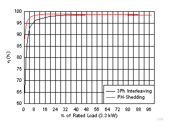 Figure 3-58 Efficiency Comparison at 230 Vrms With Phase Shedding and Without