TIDUD61E October 2020 – April 2021
- Description
- Resources
- Features
- Applications
- 5
- 1System Description
- 2System Overview
-
3Hardware, Software, Testing Requirements, and Test Results
- 3.1
Required Hardware and Software
- 3.1.1 Hardware
- 3.1.2
Software
- 3.1.2.1 Opening Project Inside CCS
- 3.1.2.2 Project Structure
- 3.1.2.3 Using CLA on C2000 MCU to Alleviate CPU Burden
- 3.1.2.4 CPU and CLA Utilization and Memory Allocation
- 3.1.2.5
Running the Project
- 3.1.2.5.1 Lab 1: Open Loop, DC (PFC Mode)
- 3.1.2.5.2 Lab 2: Closed Current Loop DC (PFC)
- 3.1.2.5.3 Lab 3: Closed Current Loop, AC (PFC)
- 3.1.2.5.4 Lab 4: Closed Voltage and Current Loop (PFC)
- 3.1.2.5.5 Lab 5: Open loop, DC (Inverter)
- 3.1.2.5.6 Lab 6: Open loop, AC (Inverter)
- 3.1.2.5.7 Lab 7: Closed Current Loop, DC (Inverter with resistive load)
- 3.1.2.5.8 Lab 8: Closed Current Loop, AC (Inverter with resistive load)
- 3.1.2.5.9 Lab 9: Closed Current Loop (Grid Connected Inverter)
- 3.1.2.6 Running Code on CLA
- 3.1.2.7
Advanced Options
- 3.1.2.7.1 Input Cap Compensation for PF Improvement Under Light Load
- 3.1.2.7.2 83
- 3.1.2.7.3 Adaptive Dead Time for Efficiency Improvements
- 3.1.2.7.4 Phase Shedding for Efficiency Improvements
- 3.1.2.7.5 Non-Linear Voltage Loop for Transient Reduction
- 3.1.2.7.6 Software Phase Locked Loop Methods: SOGI - FLL
- 3.2 Testing and Results
- 3.1
Required Hardware and Software
- 4Design Files
- 5Software Files
- 6Related Documentation
- 7About the Author
- 8Revision History
3.1.1.1 Base Board Settings
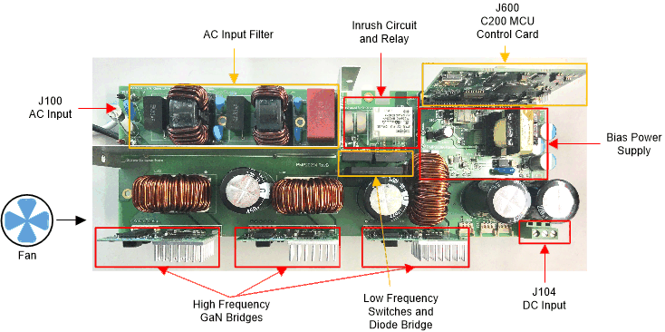
The design follows a HSEC control card concept, and any device for which HSEC control card is available from the C2000 MCU product family can be potentially used on this design. The key resources used for controlling the power stage on the MCU are listed in Table 3-1. Figure 3-1 shows the key power stage and connectors on the design board. Table 3-2 lists the key connectors and their functions. To get started:
- Make sure no power source is connected to the design.
- Insert the control card in the J600 slot.
- Connect a 12-V, 1-A DC power supply at TP604. For the ground terminal, use TP606 . Do not power up the supply.
- Connect a 5-V, 1-A DC power supply at TP608. For the ground terminal, use TP609. Do not power up the supply.
- Turn both the 12-V and 5-V power supply ON. The LED on the control card lights up and indicates the device is powered.
Note:
The bias for the MCU is separated from the power stage, which enables safe bring up of the system in this set of instructions. The bias supply design that works with this converter is PMP20396
- To connect JTAG, use a USB cable from the control card and connect it into a host computer.
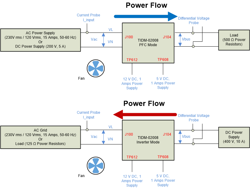
- For PFC mode, a single phase AC power supply can be connected to the input J100. Optionally in some labs a DC source may be required to test out the system safely. A resistive load of approximately 500 Ω and 400 W should be connected to the output at J104.
- For Inverter mode, A DC power supply can be connected to the input J100. A resistive load of approximately 125 Ω and 200 W should be connected to the output at J104.
- Current and voltage probes can be connected to observe the input current, input voltage, and output voltages, as shown in Figure 3-1.
 Figure 3-1 Board Overview
Table 3-1 Key Controller Peripherals Used for Control of Power Stage on Board
| SIGNAL NAME | HSEC PIN NUMBER | FUNCTION |
|---|---|---|
| PWM-1A | 49 | PWM: low-frequency MOSFET leg, high-side switch |
| PWM-1B | 51 | PWM: low-frequency MOSFET leg, low-side switch |
| PWM-2A | 53 | PWM: high frequency GaN leg, high side switch, phase one |
| PWM-2B | 55 | PWM: high-frequency GaN leg, low-side switch, phase one |
| PWM-3A | 50 | PWM: high-frequency GaN leg, high-side switch, phase two |
| PWM-3B | 52 | PWM: high-frequency GaN leg, low-side switch, phase two |
| PWM-4A | 54 | PWM: high-frequency GaN leg, high-side switch, phase three |
| PWM-4B | 56 | PWM: high-frequency GaN leg, low-side switch, phase three |
| Iac | 18 | ADC with CMPSS: AC return current measurement |
| IL1 | 15 | ADC with CMPSS : inductor current measurement Ph1 |
| IL2 | 21 | ADC with CMPSS : inductor current measurement Ph2 |
| IL3 | 25 | ADC with CMPSS : inductor current measurement Ph3 |
| VL | 20 | ADC: AC voltage line |
| VN | 17 | ADC: AC voltage neutral |
| Vbus | 24 | ADC: bus voltage |
| In Rush Relay | 57 | GPIO: used to control the inrush relay |
| GaN Fault 1 | 58 | GPIO: GaN fault signal phase one |
| GaN Fault 2 | 60 | GPIO: GaN fault signal phase two |
| GaN Fault 3 | 62 | GPIO: GaN fault signal phase three |
| AC Current Sense Gain Change | 63 | GPIO: controls the gain stage |
Table 3-2 Key Connectors and Function
| CONNECTOR NAME | FUNCTION | |
|---|---|---|
| PFC | Inverter | |
| J100 | Input AC voltage | Output AC voltage |
| J104 | Output DC bus voltage | Input DC bus Voltage |
| TP604 | Input bias supply, 12-VDC, 1 A | |
| TP608 | Input bias supply, 5-VDC, 1 A | |
| TP606/TP609 | GND | |
| J600 | HSEC control card connector slot | |
 Figure 3-2 Hardware Setup to Run Software (PFC and Inverter Mode)