TIDUD61E October 2020 – April 2021
- Description
- Resources
- Features
- Applications
- 5
- 1System Description
- 2System Overview
-
3Hardware, Software, Testing Requirements, and Test Results
- 3.1
Required Hardware and Software
- 3.1.1 Hardware
- 3.1.2
Software
- 3.1.2.1 Opening Project Inside CCS
- 3.1.2.2 Project Structure
- 3.1.2.3 Using CLA on C2000 MCU to Alleviate CPU Burden
- 3.1.2.4 CPU and CLA Utilization and Memory Allocation
- 3.1.2.5
Running the Project
- 3.1.2.5.1 Lab 1: Open Loop, DC (PFC Mode)
- 3.1.2.5.2 Lab 2: Closed Current Loop DC (PFC)
- 3.1.2.5.3 Lab 3: Closed Current Loop, AC (PFC)
- 3.1.2.5.4 Lab 4: Closed Voltage and Current Loop (PFC)
- 3.1.2.5.5 Lab 5: Open loop, DC (Inverter)
- 3.1.2.5.6 Lab 6: Open loop, AC (Inverter)
- 3.1.2.5.7 Lab 7: Closed Current Loop, DC (Inverter with resistive load)
- 3.1.2.5.8 Lab 8: Closed Current Loop, AC (Inverter with resistive load)
- 3.1.2.5.9 Lab 9: Closed Current Loop (Grid Connected Inverter)
- 3.1.2.6 Running Code on CLA
- 3.1.2.7
Advanced Options
- 3.1.2.7.1 Input Cap Compensation for PF Improvement Under Light Load
- 3.1.2.7.2 83
- 3.1.2.7.3 Adaptive Dead Time for Efficiency Improvements
- 3.1.2.7.4 Phase Shedding for Efficiency Improvements
- 3.1.2.7.5 Non-Linear Voltage Loop for Transient Reduction
- 3.1.2.7.6 Software Phase Locked Loop Methods: SOGI - FLL
- 3.2 Testing and Results
- 3.1
Required Hardware and Software
- 4Design Files
- 5Software Files
- 6Related Documentation
- 7About the Author
- 8Revision History
3.1.2.5.4.4 Running Code
- The project is programmed to wait for input voltage to excel at approximately 70 Vrms to drive the in rush relay, and clear the trip.
- Run the project by clicking
 .
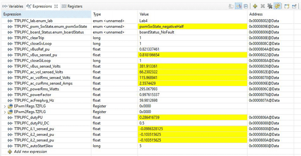
. - Now apply an input voltage of approximately 120 V. The board comes out of the undervoltage condition and inrush relay is driven. The trip clears, and the output rises to 380-V DC. A sinusoidal current is drawn from the AC input. Figure 3-28 shows the watch window when the program is running at this stage.
 Figure 3-28 Lab 4: Expressions View After AC Voltage is Applied
 - SFRA is integrated in the software of this build to verify the designed compensator provides enough gain and phase margin by measuring on hardware. To run the SFRA, keep the project running, and from the cfg page, click on the SFRA icon. SFRA GUI appears.
- Select the options for the device on the SFRA GUI. For example, for F28004x, select floating point. Click on Setup Connection, and on the pop-up window, uncheck the boot on connect option and select an appropriate COM port. Click OK. Return to the SFRA GUI, and click Connect.
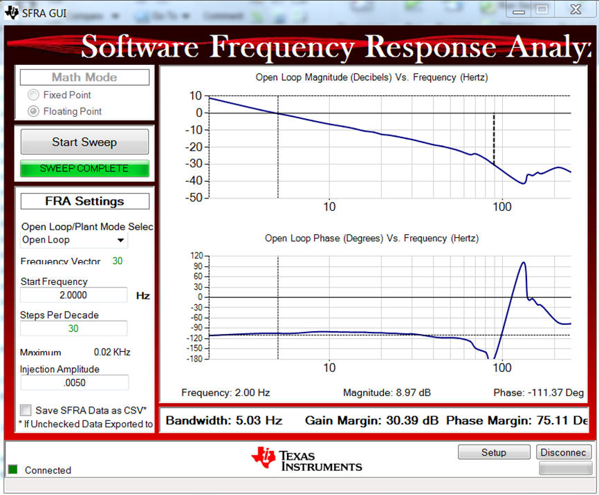
- The SFRA GUI connects to the device. A SFRA sweep can now be started by clicking Start Sweep. The complete SFRA sweep takes a few minutes to finish. Activity can be monitored by seeing the progress bar on the SFRA GUI and checking the flashing of blue LED on the back on the control card that indicates UART activity. Once complete, a graph with the open loop plot appears, as seen in Figure 3-29. This action verifies that the designed compensator is indeed stable.
 Figure 3-29 SFRA Run on Closed Voltage Loop
The frequency response data is also saved in the project folder under an SFRA data folder and is time stamped with the time of the SFRA run.
Note the measured gain and phase margin are close to the modeled values, as shown in Figure 2-12 .
- Optionally. Click on the Compensation Designer again from the CFG page, and choose SFRA Data for plant option on the GUI. This option uses the measured plant information to design the compensator, and can be used to fine tune the compensation. By default the Compensation Designer points to the latest SFRA run. If a previous SFRA run plant information must be used the user can select the SFRAData.csv file by browsing to it by clicking on Browse SFRA Data. Close the Compensation Designer to return to the cfg page once done.
- This verifies the voltage compensator design.
- To bring the system to a safe stop bring the input AC voltage down to zero, observe the TTPLPFC_vBus_sensed_Volts comes down to zero as well.
- Fully halting the MCU when in real-time mode is a two-step process. First halt the processor by using the Halt button on the toolbar (
 ) or by using Target → Halt. Then take the MCU out of real-time mode by clicking on
  . Finally, reset the MCU (
 ).
). - Close CCS debug session by clicking on Terminate Debug Session (Target → Terminate all).
