SBAU382A November 2021 – January 2022 ADS7029-Q1 , ADS7039-Q1 , ADS7040 , ADS7041 , ADS7042 , ADS7043 , ADS7044 , ADS7046 , ADS7047 , ADS7049-Q1 , ADS7052 , ADS7054 , ADS7056 , ADS7057
2.1.1 Single-Ended Input Path
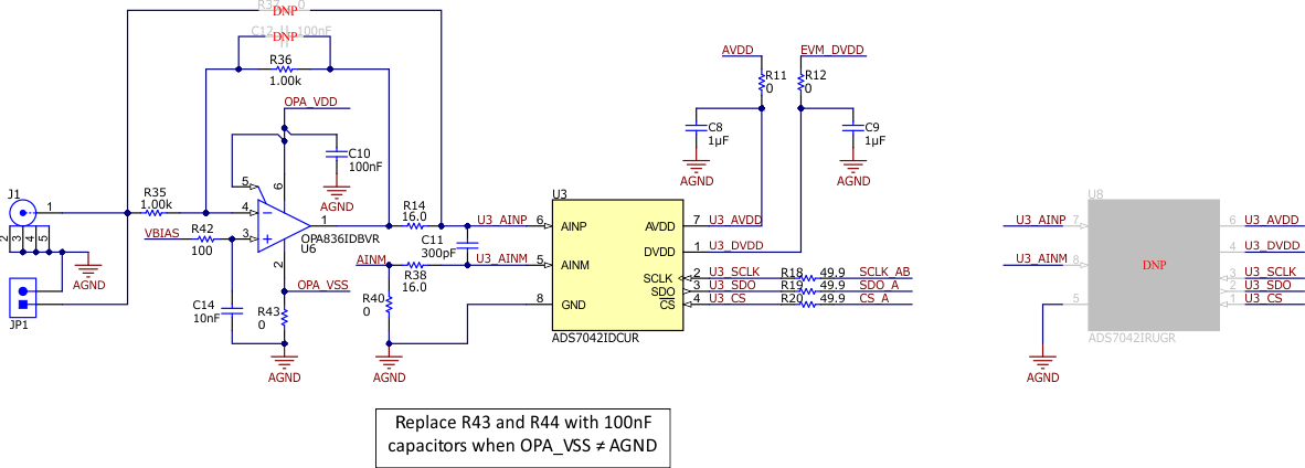
The single-ended input path consists of an inverting driver amplifier, an RC circuit, and two ADC footprints. Figure 2-2 shows the single-ended input path schematic.
 Figure 2-2 Single-Ended Input Path on the ADS704X-5XEVM
Signals connected to the single-ended input path are applied to an inverting amplifier whose common-mode voltage is set by VBIAS. The output of the amplifier connects to an RC filter (R14, R38, and C11) that then connects to the ADC input. A compensation capacitor can be added to the amplifier feedback loop via C12, but is not required for good performance. The amplifier power supplies are connected by default to the OPA_VDD and OPA_VSS supplies. Section 2.2 explains how to modify the EVM to use external supplies. If desired, the amplifier can be bypassed by populating R37 with a 0-Ω resistor and removing R14 and R35.
Figure 2-2 also depicts all connections to the ADC (U3). Each power-supply connection has a 1-μF decoupling capacitor. The supply connections also have a series 0-Ω resistor that can be removed for the purpose of making external current measurements. Moreover, each digital input has a 49.9-Ω series resistor. These resistors smooth the edges of the digital signals to minimize overshoot and ringing.
Finally, Figure 2-2 identifies a do-not-populate (DNP) component in U8. This ADC footprint is on the bottom of the board and can be used to evaluate any single-ended ADC in an X2QFN package listed in Table 1-2. However, ensure that any device in U3 is cleanly removed before soldering a device in U8. Section 4.6 explains how to use the ADS704X-5XEVM GUI to update the EEPROM when the ADC is replaced.