SBAU382A November 2021 – January 2022 ADS7029-Q1 , ADS7039-Q1 , ADS7040 , ADS7041 , ADS7042 , ADS7043 , ADS7044 , ADS7046 , ADS7047 , ADS7049-Q1 , ADS7052 , ADS7054 , ADS7056 , ADS7057
2.1.2 Differential Input Path
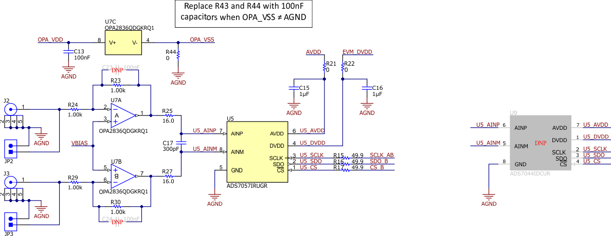
The differential input path consists of a differential driver amplifier, an RC circuit, and two ADC footprints. Figure 2-3 shows the differential input path schematic.
 Figure 2-3 Differential Input Path on the ADS704X-5XEVM
Signals connected to the differential input path are applied to a differential amplifier in an inverting configuration whose common-mode voltage is set by VBIAS. The output of the amplifier connects to an RC filter (R25, R27, and C17) that then connects to the ADC input. Each amplifier feedback loop has an option for a compensation capacitor via C23 or C24, but these capacitors are not required for good performance. The amplifier power supplies are connected by default to the OPA_VDD and OPA_VSS supplies. Section 2.2 explains how to modify the EVM to use external supplies.
Figure 2-3 also shows all connections to the ADC (U5). Each power-supply connection has a 1-μF decoupling capacitor. The supply connections also have a series 0-Ω resistor that can be removed for the purpose of making external current measurements. Moreover, each digital input has a 49.9-Ω series resistor. These resistors smooth the edges of the digital signals to minimize overshoot and ringing.
Finally, Figure 2-3 identifies a do-not-populate (DNP) component in U9. This ADC footprint is on the bottom of the board and can be used to evaluate any differential ADC in a VSSOP package in Table 1-2. However, ensure that any device in U5 is cleanly removed before soldering a device in U9. Section 4.6 explains how to use the ADS704X-5XEVM GUI to update the EEPROM when the ADC is replaced.