SBOU264B May   2021  – December 2022 INA232 , INA234 , INA236


  1.   Abstract
  2. 1Trademarks
  3. 2Overview
    1. 2.1 Kit Contents
    2. 2.2 Related Documentation From Texas Instruments
  4. 3Hardware
    1. 3.1 Features
  5. 4Operation
    1. 4.1 Quick Start Setup
    2. 4.2 EVM Operation
      1. 4.2.1 Setup
        1. 4.2.1.1 Driver Installation
        2. 4.2.1.2 Firmware
          1. 4.2.1.2.1 Firmware Debug
        3. 4.2.1.3 GUI Setup and Connection
          1. 4.2.1.3.1 Initial Setup
          2. 4.2.1.3.2 GUI to EVM Connection
      2. 4.2.2 GUI Operation
        1. 4.2.2.1 Homepage Tab
        2. 4.2.2.2 Configuration Tab
        3. 4.2.2.3 Registers Tab
        4. 4.2.2.4 Results Data Tab
      3. 4.2.3 Current Sensing Operation
        1. 4.2.3.1 Without Shunt Resistor
        2. 4.2.3.2 With Shunt Resistor
      4. 4.2.4 Direct EVM USB Communication
        1. 4.2.4.1 Standard USB CDC Read and Write Operations
        2. 4.2.4.2 Collect Data Through the USB BULK Channel
  6. 5Circuitry
    1. 5.1 Current Sensing IC
    2. 5.2 Input Signal Path
    3. 5.3 Digital Circuitry
      1. 5.3.1 I2C
  7. 6Schematics, PCB Layout, and Bill of Materials
    1. 6.1 Schematics
      1. 6.1.1 SENS079 (INA234EVM, INA236EVM)
      2. 6.1.2 SENS090 (INA232EVM)
    2. 6.2 PCB Layout
      1. 6.2.1 SENS079 (INA234EVM, INA236EVM)
      2. 6.2.2 SENS090 (INA232EVM)
    3. 6.3 Bill of Materials
      1. 6.3.1 SENS079 (INA234EVM, INA236EVM)
      2. 6.3.2 SENS090 (INA232EVM)
  8. 7Revision History

Without Shunt Resistor

To configure a measurement evaluation without a shunt resistor, follow these steps:
  1. Connect a differential voltage across the IN+ and IN– terminals (see Figure 4-14). Note that INA234EVM or INA236EVM is used for illustration. In screw terminal J1, IN+ and IN– are swapped for the INA232EVM (see Figure 4-15).
    1. If the differential voltage supply is a floating supply, connect a –0.3-V to 48-V common-mode voltage (leave powered off until finished setting up) to the inputs by connecting the positive lead of the external voltage source to either the IN+ or IN– terminal. This action effectively raises the absolute common-mode voltage of the input pins. Make sure that the differential voltage plus or minus the common-mode voltage within the –0.3-V to 48-V range.
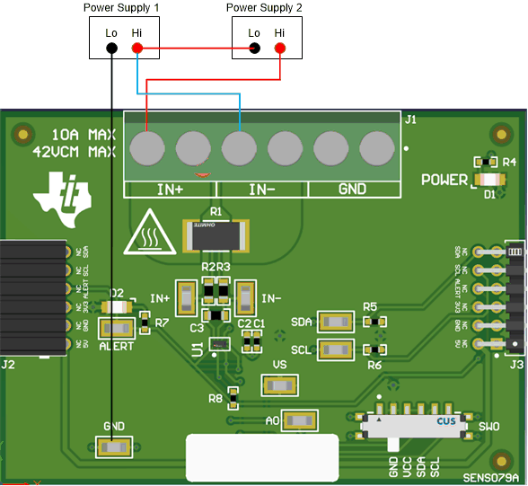
    GUID-20210423-CA0I-TNRH-VJZK-MKBNWDXK8XB6-low.gif Figure 4-14 IN+ and IN– Wiring Without a Shunt Resistor
Figure 4-15 INA232EVM
  1. Connect the VBUS terminal (J1 pin 2) to the desired bus voltage (likely either IN+ or IN–).
  2. Connect the source ground to the GND terminal (J1 pin 1).
  3. Power on the system, and observe the device states and outputs through the GUI.