SLAA957 September 2020 MSP430AFE221 , MSP430AFE222 , MSP430AFE223 , MSP430AFE231 , MSP430AFE232 , MSP430AFE233 , MSP430AFE251 , MSP430AFE252 , MSP430AFE253 , MSP430F2003 , MSP430F2013 , MSP430F2013-EP , MSP430F423A , MSP430F4250 , MSP430F425A , MSP430F4260 , MSP430F4270 , MSP430F427A , MSP430F47126 , MSP430F47127 , MSP430F47163 , MSP430F47166 , MSP430F47167 , MSP430F47173 , MSP430F47176 , MSP430F47177 , MSP430F47183 , MSP430F47186 , MSP430F47187 , MSP430F47193 , MSP430F47196 , MSP430F47197 , MSP430F477 , MSP430F478 , MSP430F4783 , MSP430F4784 , MSP430F479 , MSP430F4793 , MSP430F4794 , MSP430F6720 , MSP430F6720A , MSP430F6721 , MSP430F6721A , MSP430F6723 , MSP430F6723A , MSP430F6724 , MSP430F6724A , MSP430F6725 , MSP430F6725A , MSP430F6726 , MSP430F6726A , MSP430F6730 , MSP430F6730A , MSP430F6731 , MSP430F6731A , MSP430F6733 , MSP430F6733A , MSP430F6734 , MSP430F6734A , MSP430F6735 , MSP430F6735A , MSP430F6736 , MSP430F6736A , MSP430F6745 , MSP430F67451 , MSP430F67451A , MSP430F6745A , MSP430F6746 , MSP430F67461 , MSP430F67461A , MSP430F6746A , MSP430F6747 , MSP430F67471 , MSP430F67471A , MSP430F6747A , MSP430F6748 , MSP430F67481 , MSP430F67481A , MSP430F6748A , MSP430F6749 , MSP430F67491 , MSP430F67491A , MSP430F6749A , MSP430F67621 , MSP430F67621A , MSP430F67641 , MSP430F67641A , MSP430F6765 , MSP430F67651 , MSP430F67651A , MSP430F6765A , MSP430F6766 , MSP430F67661 , MSP430F67661A , MSP430F6766A , MSP430F6767 , MSP430F67671 , MSP430F67671A , MSP430F6767A , MSP430F6768 , MSP430F67681 , MSP430F67681A , MSP430F6768A , MSP430F6769 , MSP430F67691 , MSP430F67691A , MSP430F6769A , MSP430F6775 , MSP430F67751 , MSP430F67751A , MSP430F6775A , MSP430F6776 , MSP430F67761 , MSP430F67761A , MSP430F6776A , MSP430F6777 , MSP430F67771 , MSP430F67771A , MSP430F6777A , MSP430F6778 , MSP430F67781 , MSP430F67781A , MSP430F6778A , MSP430F6779 , MSP430F67791 , MSP430F67791A , MSP430F6779A , MSP430FE423 , MSP430FE4232 , MSP430FE423A , MSP430FE4242 , MSP430FE425 , MSP430FE4252 , MSP430FE425A , MSP430FE427 , MSP430FE4272 , MSP430FE427A , MSP430FG4250 , MSP430FG4260 , MSP430FG4270 , MSP430FG477 , MSP430FG478 , MSP430FG479 , MSP430FG6425 , MSP430FG6426 , MSP430FG6625 , MSP430FG6626 , MSP430FR5041 , MSP430FR5043 , MSP430FR50431 , MSP430FR6005 , MSP430FR6007 , MSP430FR6041 , MSP430FR6043 , MSP430FR60431 , MSP430FR6045 , MSP430FR6047 , MSP430FR60471 , MSP430I2020 , MSP430I2021 , MSP430I2030 , MSP430I2031 , MSP430I2040 , MSP430I2041
- Abstract
- Trademarks
- 1Introduction: MSP Sigma-Delta ADCs and Common Applications
- 2MSP Sigma-Delta ADC Portfolio
- 3Sigma-Delta ADC Overview
-
4MSP Sigma-Delta ADC Features
- 4.1 ADC Inputs: Differential or Single-Ended
- 4.2 Input Channels: Independent or Multiplexed
- 4.3 Integrated Buffers
- 4.4 Integrated PGAs
- 4.5 Offset Calibration: Internal or External
- 4.6 Voltage Reference: Internal or External
- 4.7 ADC Modulator Clock Frequency: Fixed or Adjustable
- 4.8 Sampling Rate versus Data Rate
- 4.9 Conversion Mode: Single or Continuous
- 4.10 Groups of ADC Channels
- 4.11 Preload
- 4.12 Output Format: Unipolar or Bipolar Data
- 4.13 Module Synchronization
- 4.14 Architecture: Discrete-Time versus Continuous-Time
- 5Solutions to Common MSP Sigma-Delta ADC Configuration Issues
- 6Frequently Asked Questions
- 7References
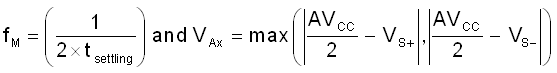
5.1.1 Settling Time Exceeds Recommended Minimum
For discrete-time SD ADC modules without integrated buffers, the source resistance of the external circuitry, the sampling capacitance (typically varies with the PGA gain setting) and the specified modulation frequency all impact the ADC settling time due to the switched-capacitor input stage. Figure 5-1 shows an analog equivalent circuit for the input stage of the SD24_B module and can be found in the Analog Input Characteristics section in the MSP430x5xx and MSP430x6xx Family User's Guide.
 Figure 5-1 Analog
Input Equivalent Circuit Example
Figure 5-1 Analog
Input Equivalent Circuit ExampleIf the actual settling time exceeds the minimum settling time for the specified modulation frequency, you may observe more noise in the digital output because the input signal does not settle completely before the next sample. The equations to calculate the minimum settling time can be found in the device-specific user's guide. For example, the minimum settling time equations for the SD24_B module are shown in Equation 1 and Equation 2 and can be found in the Analog Input Characteristics section in the MSP430x5xx and MSP430x6xx Family User's Guide.
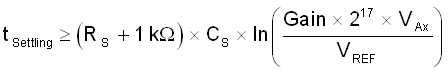
where
The resistance of the external circuit is called source resistance in MSP documentation. However, the external circuit in most designs will probably include a network of resistors, capacitors and inductors. This can cause the source resistance to vary significantly across different input frequencies, so it is referred to as source impedance in this application report.
Lowering the source impedance of the external circuitry is a change that can reduce the settling time, but this may not be feasible (for example, the design is already in production). Ideally, the impact of the external circuit on the settling time is understood during initial development. TINA-TI™ can be used to simulate the external circuit and calculate the maximum source impedance.
Lowering the sampling capacitance (reducing the PGA gain setting) is another change that can reduce the settling time, but this may not be feasible either (for example, the amplitude of the input signal is small). The sampling capacitors represent impedance because they are not purely resistive.
Lowering the modulation frequency (remember that this is the actual sampling rate of the analog signal) would be the easiest change to reduce the settling time, but this would also lower the sampling frequency (data rate).
For continuous-time SD ADC modules such as CTSD16 and SD24, the architecture does not feature a switched-capacitor input stage, so the minimum settling time does not apply. However, this does not imply that the source impedance can be infinite.