SLLA631A December 2023 – January 2024 UCC21220 , UCC21222-Q1 , UCC21520 , UCC21520-Q1 , UCC21530 , UCC21530-Q1 , UCC21540 , UCC21540-Q1
- 1
- Abstract
- Trademarks
- 1Introduction
- 2When Can Extreme Narrow Input Pulses Happen in a Power Stage?
- 3How Narrow Input Pulse Widths Threaten the Gate Driver
- 4Which System Factors Can Influence the Result
- 5How do you Know Whether Your System Should Limit Narrow Pulses?
- 6Summary
- 7References
- 8Revision History
3 How Narrow Input Pulse Widths Threaten the Gate Driver
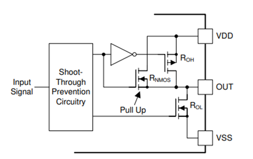
Gate drivers sink and source current when switching the gate of a MOSFET. There’s a pull-up and pull-down structure inside the device, which buffers the input signal and provides sufficient current to charge and discharge the gate capacitance. Figure 3-1 shows an example of an output structure where a parallel combination of a PMOS and NMOS device enable the output for the gate driver.
 Figure 3-1 Example Gate Driver Output
Stage (for one Channel)
Figure 3-1 Example Gate Driver Output
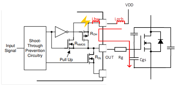
Stage (for one Channel)In the narrow ON pulse scenario, the MOSFET turn-on procedure has not completed when the driver receives the OFF command, and the internal totem-pole pull-up stage is still continually conducting a very high current (IG >> 0).
In a real-world gate drive circuit, the inductance Lpcb of Figure 3-2 in series with VDD can be large due to parasitic PCB trace inductance. When combined with internal driver parasitic inductance from the bond wires, the total inductance on at VDD can often be over 10nH. When the drive current suddenly gets cut off, a large parasitic inductance can cause significant voltage spikes (Vspike= L di/dt), which can lead to voltage exceeding the recommended operating conditions, even going beyond the absolute maximum rating in some cases.
 Figure 3-2 Gate Turn on Current Path and
Parasitic
Figure 3-2 Gate Turn on Current Path and
ParasiticAs discussed in the previous section, the gate driver can experience a short input pulse width at every AC zero crossing for a typical totem pole PFC circuit. In the end equipment lifetime, narrow pulse events can happen hundreds of millions of times. Therefore, narrow input pulses can become a hidden risk for a project. Exceeding the maximum VDD or VOUT voltage might not lead to a sudden failure during the project development phase, but repetitive operating outside device SOA can cause early degradation and premature damage of a gate driver.
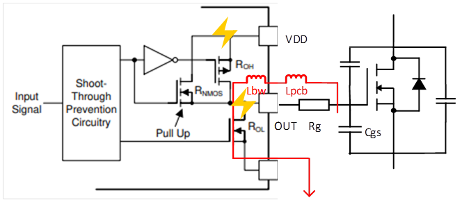
Similarly, the narrow OFF input pulse (close to 100% duty) might also lead to overstress of OUT and VDD. In the narrow OFF pulse scenario, the MOSFET turn-off procedure has not completed when the driver receives the ON command, and the internal totem-pole pull-down stage is still continually conducting very high current (IG >> 0). The large parasitic inductance and sudden current change can cause significant voltage spikes on output pin. When the OUT voltage is higher than VDD voltage, it can further stress the VDD pin as well.
 Figure 3-3 Gate Turn Off Current Path and
Parasitic