SLLSFB7 March 2026 TLIN1124A-Q1
ADVANCE INFORMATION
- 1
- 1 Features
- 2 Applications
- 3 Description
- 4 Pin Configuration and Functions
- 5 Specifications
- 6 Parameter Measurement Information
-
7 Detailed Description
- 7.1 Overview
- 7.2 Functional Block Diagram
- 7.3 Feature Description
- 7.4 Device Functional Modes
- 8 Application and Implementation
- 9 Device and Documentation Support
- 10Revision History
- 11Mechanical, Packaging, and Orderable Information
4 Pin Configuration and Functions
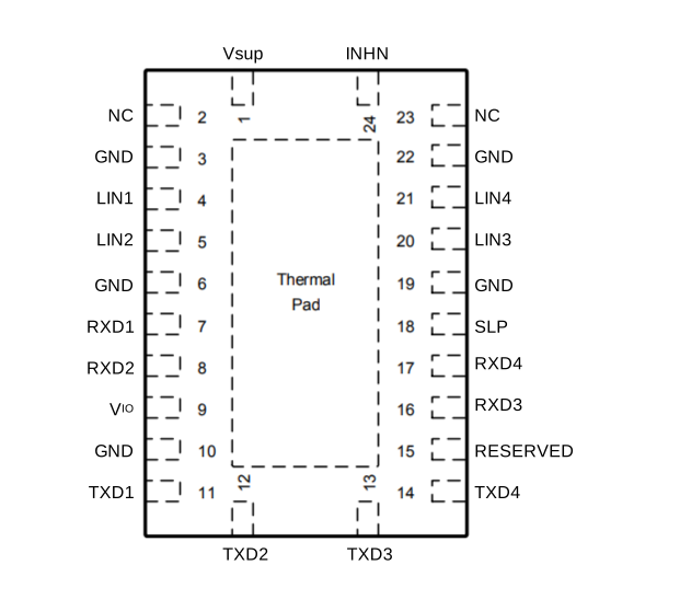 Figure 4-1 RGY Package, 24-Pin (VQFN)
Top View
Table 4-1 Pin Functions
| PIN(1) | TYPE | DESCRIPTION | |
|---|---|---|---|
| NO. | NAME | ||
| 1 | VSUP | Power | High voltage supply from battery |
| 2 | |||
| NC | - | Not connected | |
| 3 | GND | GND | Ground |
| 4 | LIN1 | Bus I/O | Channel 1 LIN Bus single-wire transmitter and receiver |
| 5 | LIN2 | Bus I/O | Channel 2 LIN Bus single-wire transmitter and receiver |
| 6 | GND | GND | Ground |
| 7 | RXD1 | Digital Output | Channel 1 RXD Output (push-pull) interface reporting state of LIN1 bus |
| 8 | RXD2 | Digital Output | Channel 2 RXD Output (push-pull) interface reporting state of LIN2 bus |
| 9 | VIO | Power | Logic interface supply voltage |
| 10 | GND | GND | Ground |
| 11 | TXD1 | Digital Input | Channel 1 TXD input interface to control state of LIN1 output; integrated weak pull-down and pull-up; |
| 12 | TXD2 | Digital Input | Channel 2 TXD input interface to control state of LIN2 output; integrated weak pull-down and pull-up; |
| 13 | TXD3 | Digital Input | Channel 3 TXD input interface to control state of LIN3 output; integrated weak pull-down and pull-up; |
| 14 | TXD4 | Digital Input | Channel 4 TXD input interface to control state of LIN4 output; integrated weak pull-down and pull-up; |
| 15 | RESERVED | Digital Input | For normal operation. This pin must be driven low or connected to GND |
| 16 | RXD3 | Digital Output | Channel 3 RXD Output (push-pull) interface reporting state of LIN3 bus |
| 17 | RXD4 | Digital Output | Channel 4 RXD Output (push-pull) interface reporting state of LIN4 bus |
| 18 | SLP | Digital input | Logic input to control state of LIN channels, integrated pull-up to VIO |
| 19 | GND | GND | Ground |
| 20 | LIN3 | Bus I/O | Channel 3 LIN Bus single-wire transmitter and receiver |
| 21 | LIN4 | Bus I/O | Channel 4 LIN Bus single-wire transmitter and receiver |
| 22 | GND | GND | Ground |
| 23 | NC | - | Not connected |
| 24 | INHN | High voltage output | Inhibit output to control system voltage, high voltage. Active low, open drain. |
| PAD | Thermal pad | - | Must be grounded on PCB for optimum thermal performance |
(1) Pin 3, 6, 10, 19 and 22: All GND pins are shorted internally.