SLLU312A July 2019 – May 2022 TCAN4550-Q1
- TCAN4550-Q1 Functional Safety-Manual
- Trademarks
- 1Introduction
- 2Product Functional Safety-Capability
- 3Product Overview
- 4Development Process for Management of Systematic Faults
- 5Revision History
3.2.1.5 CAN Bus Communication
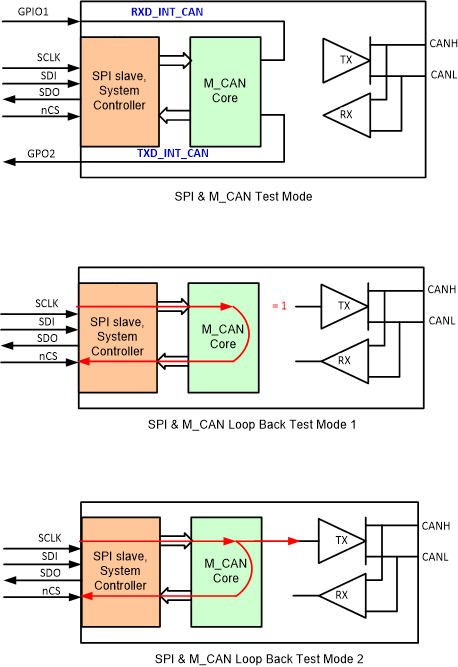
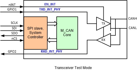
CAN bus communication, shown as fault 2, is a main concern in a system. This can happen due to many different mechanisms. Some have been covered in the previous sections of this document. The Bosch M_CAN core has a CRC checker that validates the CAN data so corrupted data does not get transferred to the node processor from the bus. The M_CAN core also provide two loop back test modes that allow the implementer to determine if the data transmitted and received through the core are the same; see Figure 3-8 loop back test mode 1 and 2. These three SPI↔M_CAN test modes are safety mechanism SM-07, SM-08 and SM-09. If an error is detected there are two other test modes that can be used to determine if the error is in the digital core or the transceiver; see Figure 3-8 and Figure 3-9. Driver and receiver function test modes map the internal TXD_INT_PHY, RXD_INT_PHY and EN_INT signals to GPIO to drive and receive data to CAN bus. Table 3-5 and Table 3-6 provide information on CAN bus state when using transceiver test mode and is considered safety mechanism SM-10. Diagnostic tools like dominant state timeout which makes sure the bus is not stuck dominant if the TXD_INT_PHY signal is stuck low. The M_CAN signals TXD_INT_CAN and RXD_INT_CAN can be mapped to GPIO as an aid in diagnostic to determine if the expected data is transmitted from SPI through M_CAN core and vise versa. Table 3-5 and Table 3-6 provide information on CAN bus state when using transceiver test mode.
The TCAN4550-Q1 provides CAN bus short circuit current limiting and is considered safety mechanism SM-06. These also mitigate potential faults 4 and 8.
| DEVICE MODE | TXD_INT INPUT | BUS OUTPUTS | DRIVEN BUS STATE | |
|---|---|---|---|---|
| CANH | CANL | |||
| Normal | L | H | L | Dominant |
| H or Open | Z | Z | Biased Recessive | |
| Standby | X | Z | Z | Weak Pull to GND |
| Sleep | X | Z | Z | Weak Pull to GND |
| DEVICE MODE | CAN DIFFERENTIAL INPUTS VID = VCANH – VCANL | BUS STATE | RXD_INT TERMINAL |
|---|---|---|---|
| Normal | VID ≥ 0.9 V | Dominant | L |
| 0.5 V < VID < 0.9 V | Undefined | Undefined | |
| VID ≤ 0.5 V | Recessive | H | |
| Standby/Sleep | VID ≥ 1.15 V | Dominant | See TCAN4550-Q1 data sheet figure 24 for more detial |
| 0.4 V < VID < 1.15 V | Undefined | ||
| VID ≤ 0.4 V | Recessive | ||
| Any | Open (VID ≈ 0 V) | Open | H |
 Figure 3-8 SPI and M_CAN Test Modes
 Figure 3-9 CAN Transceiver Test Mode