SLLU312A July   2019  – May 2022 TCAN4550-Q1


  1.   TCAN4550-Q1 Functional Safety-Manual
  2.   Trademarks
  3. 1Introduction
  4. 2Product Functional Safety-Capability
  5. 3Product Overview
    1. 3.1 Block Diagram
    2. 3.2 Target Applications
      1. 3.2.1 Diagnostic Features
        1. 3.2.1.1 Mode Overview
        2. 3.2.1.2 Sleep Wake Error Timer (SWE)
        3. 3.2.1.3 Undervoltage
        4. 3.2.1.4 Thermal Shut Down
        5. 3.2.1.5 CAN Bus Communication
          1. 3.2.1.5.1 M_CAN
        6. 3.2.1.6 Processor Communication
          1. 3.2.1.6.1 SPI Integrity
            1. 3.2.1.6.1.1 SPI Scratchpad
            2. 3.2.1.6.1.2 SPIERR
            3. 3.2.1.6.1.3 M_CAN Forced Dominant and Recessive
            4. 3.2.1.6.1.4 SPI and FIFO
            5. 3.2.1.6.1.5 ECC for Memory
          2. 3.2.1.6.2 Timeout Watchdog
          3. 3.2.1.6.3 Floating Pins
          4. 3.2.1.6.4 RST Pin
          5. 3.2.1.6.5 Interrupt and Internal Fault Detection
  6. 4Development Process for Management of Systematic Faults
    1. 4.1 TI New-Product Development Process
  7. 5Revision History

Block Diagram

The TCAN4550-Q1 is a mixed signal device containing both analog and digital cores. The device integrates the Bosch M_CAN revision 3.2.1.1 controller which is not covered in this document. Figure 3-2 and Figure 3-3 are the high level mixed signal and digital core functional block diagrams. CCLK is internally connected to the crystal/CLKIN.
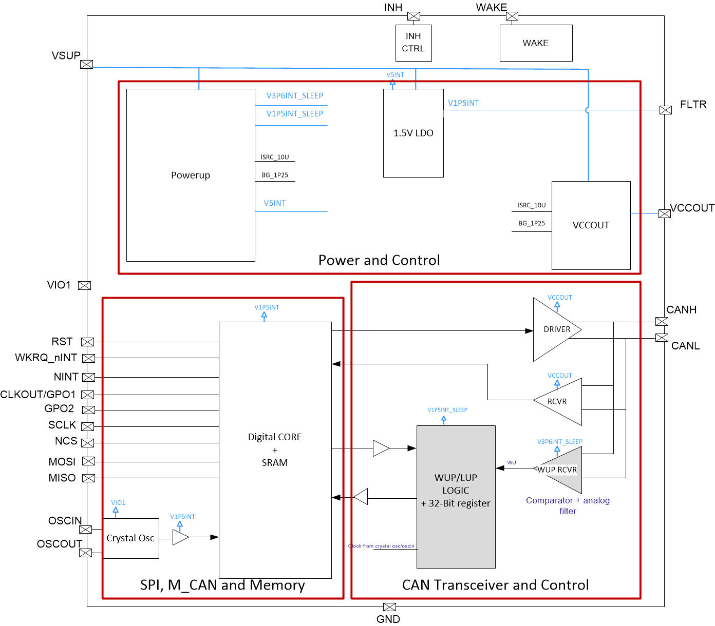
GUID-CD00A9FA-DEC3-4026-9CE0-5AA5E8A1C973-low.gifFigure 3-2 TCAN4550-Q1 Mixed Signal Functional Block Diagram
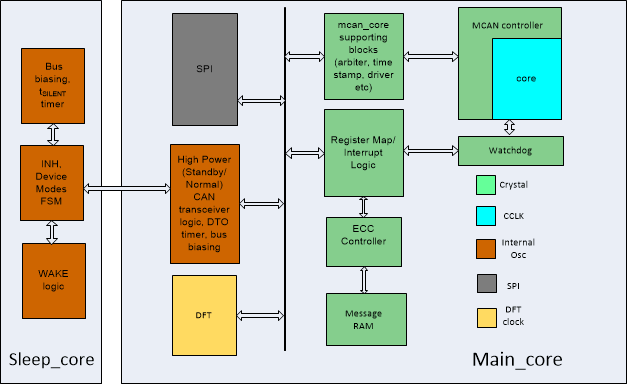
GUID-E6E54104-C25E-413C-8938-1DEFC7B974B9-low.gifFigure 3-3 Digital Core Block Diagram and Clock Tree