SLOA059B October 2022 – March 2023 OPA2991 , TLC2654 , TLC4502 , TLE2021 , TLV2721
5.3 Specifications
The very name input offset voltage indicates that it has been referred to the op amp input. This is done with all of the error sources because the actual output created by any error source depends on the closed-loop gain (ACL) of the circuit, as seen from the error source. Thus, VOS must be multiplied by the non-inverting circuit's ACL to be referenced to the output.
| PARAMETER | TEST CONDITIONS | MIN | TYP | MAX | UNIT | ||
|---|---|---|---|---|---|---|---|
| OFFSET VOLTAGE | |||||||
| VOS | Input offset voltage | OPA991, OPA2991 VCM = V– |
±125 | ±750 | µV | ||
| TA = –40°C to 125°C | ±780 | ||||||
| OPA4991 VCM = V– |
±125 | ±830 | |||||
| TA = –40°C to 125°C | ±850 | ||||||
| dVOS/dT | Input offset voltage drift | TA = –40°C to 125°C | ±0.3 | µV/℃ | |||
The designator comes after the part name and before the package name.
| Designator | Ambient Temperature Range | Designator Meaning |
|---|---|---|
| C | 0°C to 70°C | Commercial |
| I | -40°C to 85°C | Industrial |
| T | -40°C to 105°C | N/A |
| Q | -40°C to 125°C | Automotive |
| E | -40°C to 150°C | Extended |
| M | -55°C to 125°C | Military |
Table 5-1 shows the VOS portion of the OPA2991 data sheet. Each VOS specification has a column on the data sheet for the minimum, typical, and maximum values to be listed. There are three major VOS specifications that may be provided for an op amp: VOS at 25°C, VOS full range, and drift over temperature (ΔVOS/ΔT). In the past, devices fell under specific operating temperature ranges with letter designators as shown in Table 5-2. However, most new devices have a temperature range from –40°C to +125°C regardless of application. Some devices are also marked with letters such as A or B. These grades indicate the accuracy of the part—the better the quality (grade), the lower the DC errors. This is not always the case, so always check the data sheet for the actual VOS specifications.
The first entry is for VOS under static temperature conditions, where the maximum and typical values are listed for a temperature of 25°C. This specification is listed on virtually all op amp data sheets and is expressed in millivolts (mV) or microvolts (μV). It is possible that natural variations or future changes in the process used to create a device result in a VOS that is much different from the typical value. Every device is tested at the factory to ensure that it does not exceed the maximum specified value before it is shipped to the customer, so a robust design may require a designer to look at maximum instead of typical values.
On a data sheet, VOS full range is usually only provided with a maximum rating. This specification lists the worst possible VOS that can be encountered over a specified temperature range. Occasionally, the full range is specified for a temperature range less than the maximum operating temperature range, so strict attention must be paid to the conditions.
The drift of a device with temperature is indicated by ΔVOS/ΔT. This is an average that is calculated using the ends of the specified temperature range as shown in Equation 13. For example, VOS for many parts is measured at –40°C (TA1) and 125°C (TA2) and the results are calculated and expressed as the number of microvolts of increase in VOS per degree Celsius of temperature change (μV/°C). Drift is usually given as a typical value on data sheets. Note that only maximum values are production tested by TI, so look at the full range data or measure drift to get a more complete understanding of the device's drift.
Some devices have multiple slopes in their drift plot, so Equation 14 is used. This is useful when there are different slopes in different regions, since a calculation over the whole range would show only a small drift when there could be larger drifts which cancel.
Figure 5-2 shows VOS measured from –40°C to 125°C (a typical temperature range) for several devices and compares the VOS drift behavior. The slope of each line indicates the magnitude of drift, or ΔVOS/ΔT, for that part. The steeper the line, the greater the ΔVOS/ΔT. The OPA2991 is shown to have less drift over temperature as compared to the LM358B. A designer should consider the full drift range behavior if temperature variance is expected in the application.
 Figure 5-2 VOS Drift Over Temperature
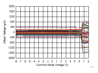
Figure 5-3 and Figure 5-4 is an example of the relationship between VOS and the input common mode voltage (VCM) using TLV9161, OPAx991, and TLV07xH. Since VOS is normally tested at one value of VCM, such graphs are useful in inferring behavior that is not specified in the data sheet. They provide the designer with an understanding of the behavior of the device over a wide range of values.
 Figure 5-3 VOS vs. VCM for the TLV9161 Op Amp
 Figure 5-4 VOS vs. VCM for the OPAx991 (Left) and the TL07xH (Right)