SLUUCD4 April 2021 TPS92682-Q1
- Trademarks
- General Texas Instruments High Voltage Evaluation (TI HV EMV) User Safety Guidelines
- 1Description
- 2REACH Compliance
- 3Performance Specifications
- 4Performance Data and Typical Characteristic Curves
- 5Schematic, PCB Layout, and Bill of Materials
- 6Software
- 7TPS92682EVM-125 Power UP and Operation
5.2 Layout
The TPS92682EVM-125 is a four-layer board. Figure 5-2, Figure 5-3, Figure 5-4, Figure 5-5, and Figure 5-6 illustrate the assembly, the top, the inner-layer1, the inner-layer2 and the bottom layer of the TPS92682EVM-125 PCB layout.
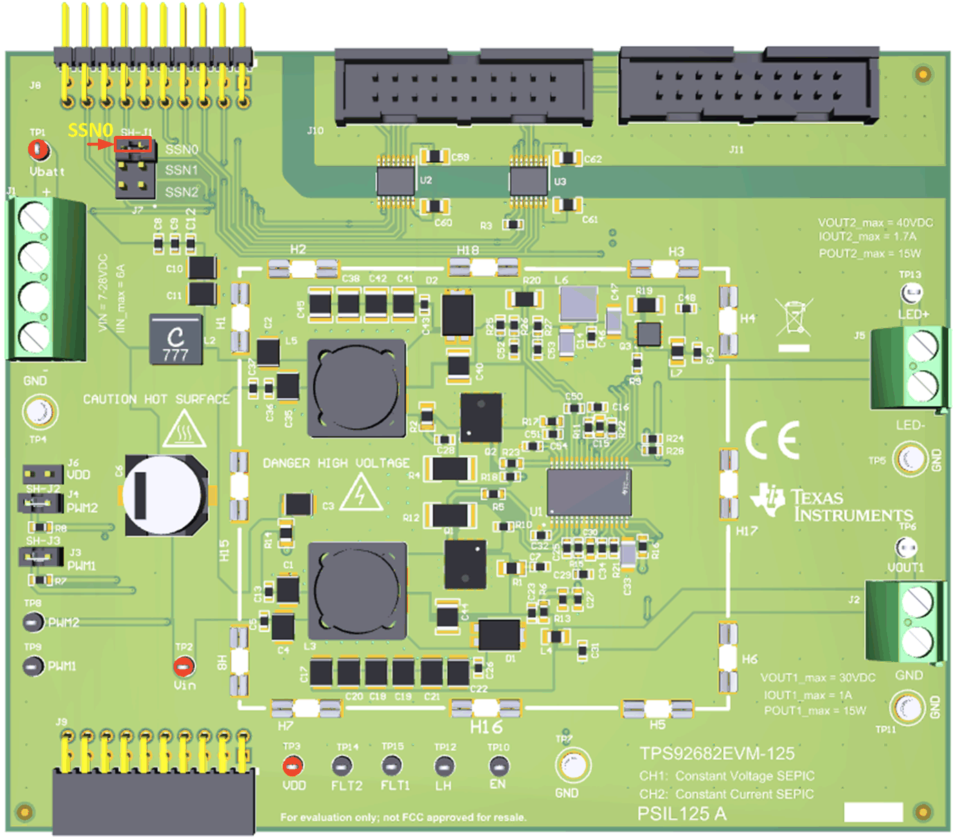 Figure 5-2 TPS92682EVM-125 Assembly
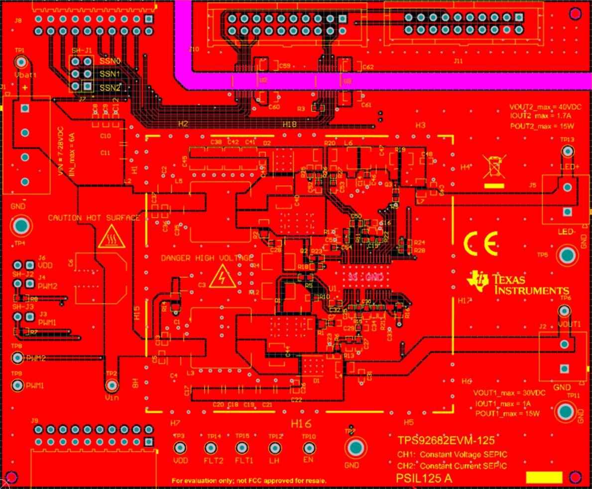 Figure 5-3 TPS92682EVM-125 Top Layer and Top Overlay (Top View)
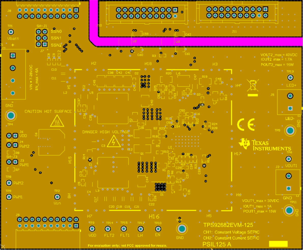 Figure 5-4 TPS92682EVM-125 Inner-layer 1
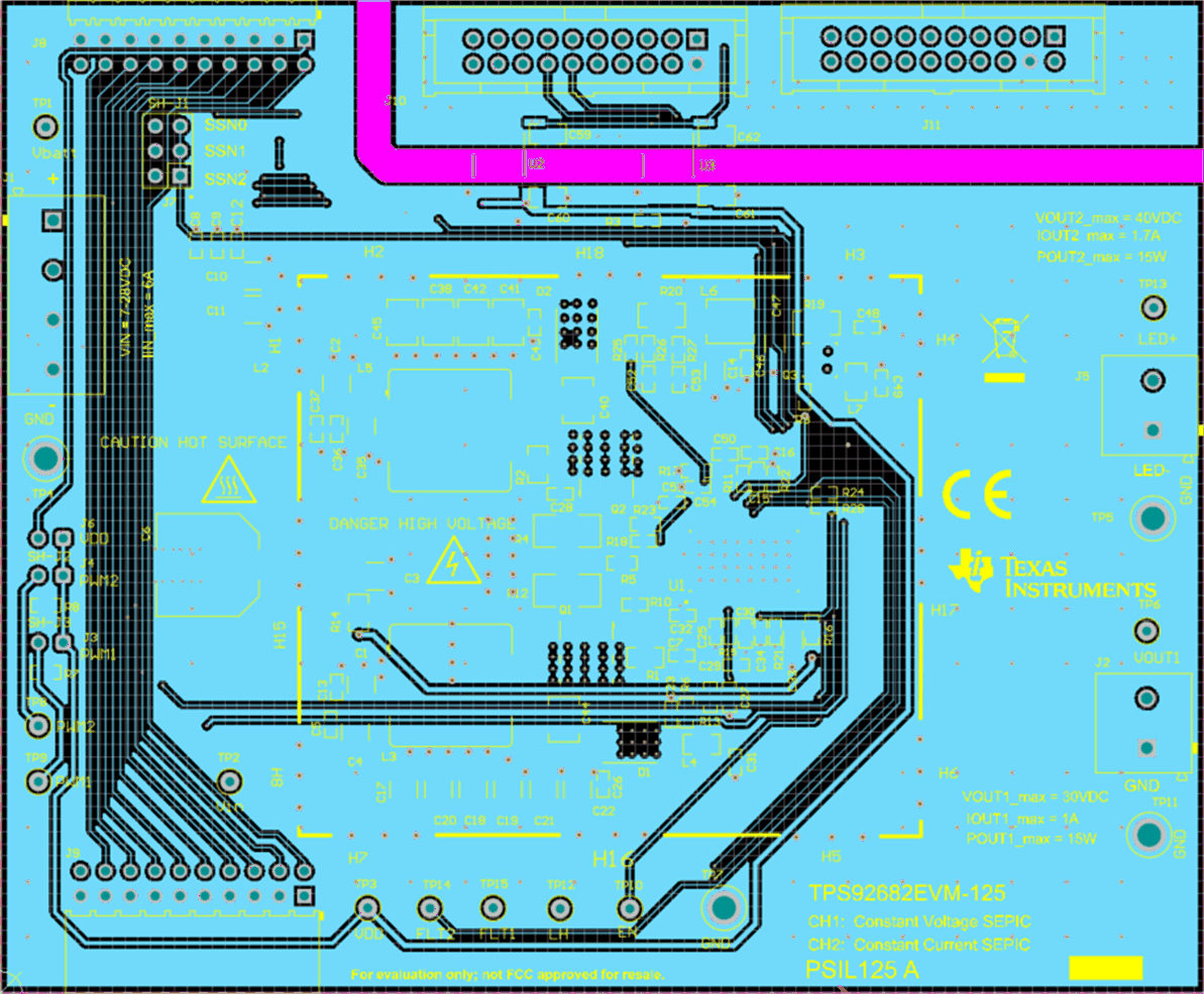 Figure 5-5 TPS92682EVM-125 Inner-layer 2
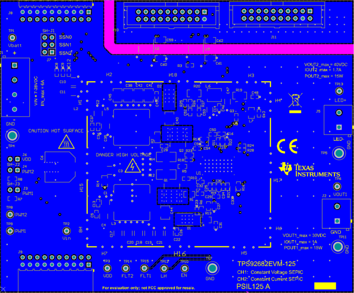 Figure 5-6 TPS92682EVM-125 Bottom Layer (Bottom View)