SLUUCD4 April 2021 TPS92682-Q1
- Trademarks
- General Texas Instruments High Voltage Evaluation (TI HV EMV) User Safety Guidelines
- 1Description
- 2REACH Compliance
- 3Performance Specifications
- 4Performance Data and Typical Characteristic Curves
- 5Schematic, PCB Layout, and Bill of Materials
- 6Software
- 7TPS92682EVM-125 Power UP and Operation
1.3 Connector Description
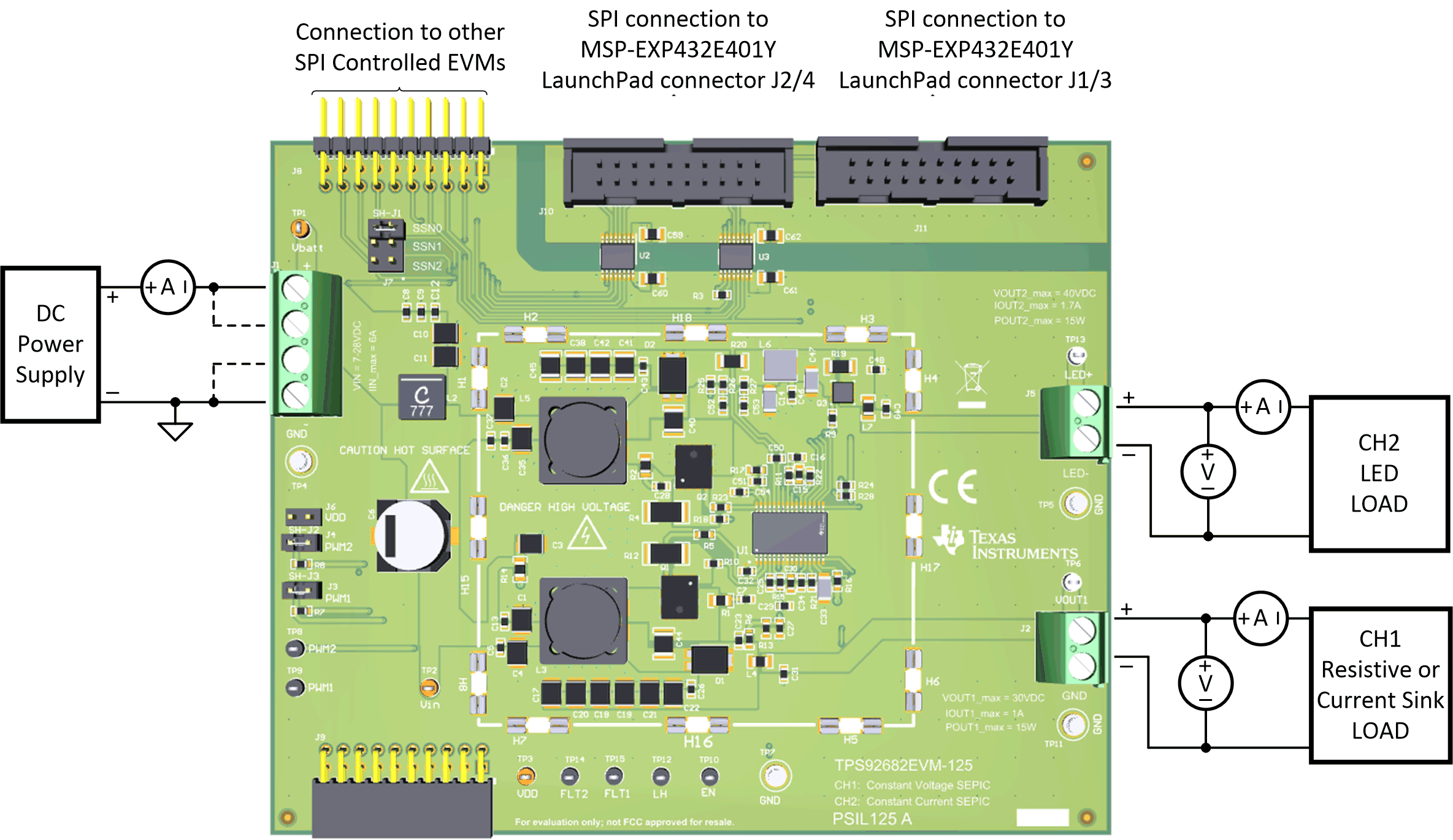
Table 1-1 describes the connectors and Table 1-2 lists the test points on the EVM and how to properly connect, set up, and use the TPS92682EVM-125.Figure 1-1 shows the connection diagram and the default jumper locations of the TPS92682EVM-125.
 Figure 1-1 Component Connections
Table 1-1 Connector Descriptions
| Connector | Label | Description |
|---|---|---|
| J10 | SPI control from the MSP-EXP432E401Y LaunchPad | J10 and J11 allow attachment of a header cable for SPI control of the TPS92682-Q1 to the TI SimpleLink™ Ethernet MSP-EXP432E401Y MCU LaunchPad™ Development Kit, part number MSP-EXP432E401Y |
| J11 | ||
| J8 | SPI control signals to other SPI controlled EVM | J8 and J9 allow star connection of TPS92682EVM-125 boards to each other with one MSP-EXP432E401Y control board. |
| J9 | ||
| J1 | VIN, GND | J1 connects the input power to the TPS92682EVM-125. The board silkscreen identifies VIN pins with "Vbatt" and the "GND" markings. |
| J2 | Channel-1 and Channel-2 and GND | J2 is connected to the channel-1 output and J5 is connected to the channel-2 output of the TPS92682EVM-125. |
| J5 | ||
| J6 | VDD jumper | J6 is a jumper provided to share VDD with other SPI controlled EVM, in case a digital supply is needed. For the operation of this EVM, leave this jumper open. |
| J3 | PWM1 and PWM2 jumpers | J3 and J4 are jumpers to apply external PWM signals to the two channels. When the jumpers are removed and the R28 and R29 resistors are installed, the PWM signals can be generated from the MSP-EXP432E401Y controller board. When the jumpers are populated (by default), the PWM1 and PWM2 pins of the TPS92682-Q1 are connected to VDD. |
| J4 | ||
| J7 | SSN configuration jumper | J7 allows configuration of the SSN chip select line, when multiple chips on the same SPI bus are used. By default, evaluation module is configured to be connected to the SSN0 of the MSP-EXP432E401Y controller board. |
Table 1-2 Test Points
| Test Point | Description |
|---|---|
| Metal turrets | All metal turrets are grounds. |
| Vbatt | The VBAT test point allows for voltage measurement of the external power supply applied to the evaluation board. |
| Vin | The VIN test point allows for voltage measurement of the power applied to the boost and boost-to-battery channels after the EMI filter. |
| VDD | The VDD test point allows for voltage measurement of the VDD output of the TPS92682-Q1. |
| LH | The LH test point allows for applying a voltage to the LH pin and placing the TPS92682-Q1 in Limp Home mode |
| FLT1 | The FLT1 test point can be used to monitor the fault occurrence of the channel-1. When a fault occurs, FLT1 voltage level goes low. Note that during power up, FLT1 is low (due to POR). The Fault pins can be reset by setting bit-7 of the EN register 0x00. |
| FLT2/SYNC | The FLT2 test point can be used to monitor the fault occurrence of the channel-2. When a fault occurs, FLT2 voltage level goes low. Note that during power up, FLT2 is low (due to POR). The Fault pins can be reset by setting bit-7 of the EN register 0x00. The FLT2 test point can also be used for synchronizing of the TPS92682-Q1 with an external clock. |
| EN | EN test point is connected to the EN-pin of the TPS92682-Q1 device |
| PWM1 | PWM1 test point is connected to the PWM1-pin of the TPS92682-Q1 device |
| PWM2 | PWM2 test point is connected to the PWM2-pin of the TPS92682-Q1 device |
| LED+ | The LED+ test point allows for voltage measurement of the channel-2 LED positive output. |
| LED- | The LED- test point is connected to the channel-2 LED negative output. This test point is connected to the EVM ground plane |
| Vout1 | The Vout1 test point is connected to the channel-1 CV regulator. |