SLUUD38A June   2024  – July 2025 TPSM82866A , TPSM82866C


  1.   1
  2.   Description
  3.   Features
  4.   4
  5. 1Evaluation Module Overview
    1. 1.1 Introduction
    2. 1.2 Kit Contents
    3. 1.3 Specification
    4. 1.4 Device Information
  6. 2Hardware
    1. 2.1 Safety Instructions
    2. 2.2 Header Information
    3. 2.3 Jumper Information
    4. 2.4 Interfaces
    5. 2.5 Test Points
  7. 3Software
  8. 4Implementation Results
    1. 4.1 Evaluation Setup
      1. 4.1.1 VSET/VID Resistor (TPSM82866CAxPEVM Only)
      2. 4.1.2 VSET/MODE Resistor (TPSM82866AA0PEVM Only)
      3. 4.1.3 Input and Output Capacitors
      4. 4.1.4 Feedforward Capacitor
      5. 4.1.5 Loop Response Measurement
    2. 4.2 Performance Data and Results
  9. 5Hardware Design Files
    1. 5.1 Schematics
    2. 5.2 PCB Layout
    3. 5.3 Bill of Materials (BOM)
  10. 6Additional Information
    1. 6.1 Revision A EVMs
      1. 6.1.1 Rev A. Schematic
      2. 6.1.2 Rev. A Bill of Materials (BOM)
      3. 6.1.3 Rev. A PCB Layout
      4. 6.1.4 Rev. A Loop Response
    2. 6.2 Trademarks
  11. 7Revision History

PCB Layout

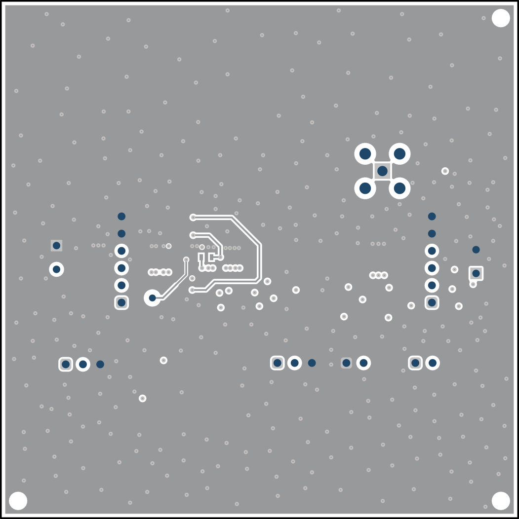
This section provides the TPSM82866 EVM board layout (SR054). The Gerber files are available on the TPSM82866AA0PEVM tool folder. All four layers use 2-ounce copper.

TPSM82866AA0PEVM, TPSM82866CA1PEVM, TPSM82866CA2PEVM, TPSM82866CA3PEVM Top AssemblyFigure 5-5 Top Assembly
TPSM82866AA0PEVM, TPSM82866CA1PEVM, TPSM82866CA2PEVM, TPSM82866CA3PEVM Internal Layer 1Figure 5-7 Internal Layer 1
TPSM82866AA0PEVM, TPSM82866CA1PEVM, TPSM82866CA2PEVM, TPSM82866CA3PEVM Bottom LayerFigure 5-9 Bottom Layer
TPSM82866AA0PEVM, TPSM82866CA1PEVM, TPSM82866CA2PEVM, TPSM82866CA3PEVM Top LayerFigure 5-6 Top Layer
TPSM82866AA0PEVM, TPSM82866CA1PEVM, TPSM82866CA2PEVM, TPSM82866CA3PEVM Internal Layer 2Figure 5-8 Internal Layer 2
TPSM82866AA0PEVM, TPSM82866CA1PEVM, TPSM82866CA2PEVM, TPSM82866CA3PEVM Bottom Assembly (Mirrored)Figure 5-10 Bottom Assembly (Mirrored)