SLVAEI5A december   2019  – june 2023 TPS25830-Q1 , TPS25830A-Q1 , TPS25831-Q1 , TPS25840-Q1


  1.   1
  2.   TPS25830, TPS25831-Q1, and TPS25840-Q1 Short-to-Battery Application
  3.   Trademarks
  4. 1Introduction
  5. 2Short-to-Battery Conventional Application
    1. 2.1 External FET VBUS/DP_IN/DM-IN Short-to-VBAT Application
      1. 2.1.1 VBUS Short-to-VBAT Application
      2. 2.1.2 DP_IN/DM_IN Short-to-VBAT Application
      3. 2.1.3 VBUS /DP_IN/DP_IN Short-to-VBAT Application Summary
    2. 2.2 Without External FET VOUT/DP_IN/DM-IN Short-to-VBAT Application
      1. 2.2.1 VOUT/CSN Short-to-VBAT Application
      2. 2.2.2 DP_IN/DM_IN Short-to-VBAT Application
      3. 2.2.3 VOUT/DP_IN/DP_IN Short-to-VBAT Application Summary
    3. 2.3 CC1/CC2 Short-to-VBAT Application
  6. 3Short-to-Battery Special Application
    1. 3.1 External FET VBUS/DP_IN/DM-IN Short-to-VBAT Application
      1. 3.1.1 VBUS Short-to-VBAT Application
      2. 3.1.2 DP_IN/DM_IN Short-to-VBAT Application
      3. 3.1.3 VBUS/DP_IN/DM-IN Short-toVBAT Application Summary
    2. 3.2 Without External FET VOUT/DP_IN/DM-IN Short-to-VBAT Application
      1. 3.2.1 VOUT Short-to-VBAT Application
      2. 3.2.2 DP_IN/DM_IN Short-to-VBAT Application
      3. 3.2.3 VOUT /DP_IN/DM-IN Short-to-VBAT Application Summary
  7. 4Short-to-Battery Connect to TVS Application
    1. 4.1 VBUS Short-to-VBAT Connect to TVS Application
    2. 4.2 VOUT Short-to-VBAT Connect to TVS Application
    3. 4.3 DP/DM Short-to-VBAT Connect to TVS Application
    4. 4.4 CC1/CC2 Short-to-VBAT Connect to TVS Application
  8. 5Revision History

DP_IN/DM_IN Short-to-VBAT Application

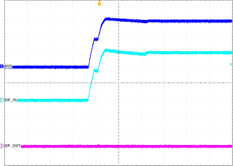
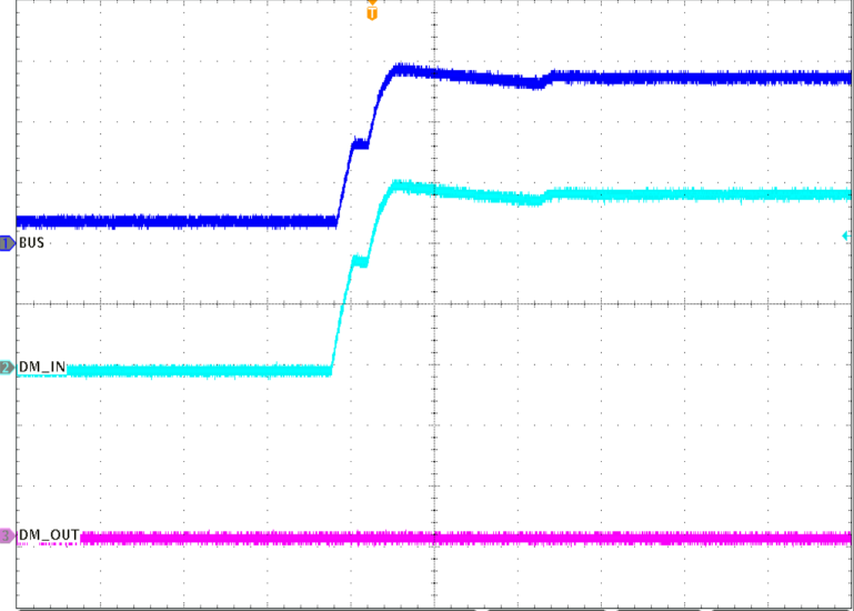
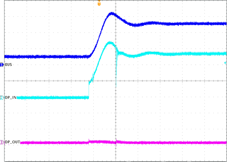
Application 1: Figure 3-1 shows the test setup. The state at each point is power supply off (Vout = 0 V, LS_GD is low, and Q1 is off). Short DP_IN/DM_IN to VBAT. The voltage of DP_IN/DM_IN rushes to the same height as VBAT. Figure 3-7 and Figure 3-8 show the test results.

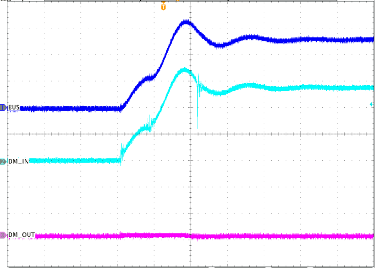
Application 2: Figure 3-2 shows the test setup. DP_IN/DM_IN shorts to VBAT. The input voltage and DP_IN/DM_IN voltage are rushed to the same height as VBAT together. Figure 3-9 and Figure 3-10 show the test results.

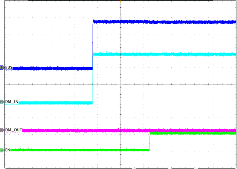
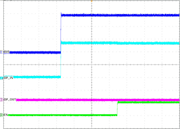
Application 3: Figure 3-3 shows the test setup. First, short DP_IN/DM_IN to VBAT and power on the power supply, then enable EN. Figure 3-11 and Figure 3-12 show the test results.
GUID-8A3B76EF-B20A-425E-A6FD-3AD6FE583840-low.png
CH1 = 5 V/div, CH2 = 5 V/div, CH3 = 5 V/div, 2 µS/div
Figure 3-7 Power Off, DP_IN Short-to-VBAT Test
GUID-1D527B87-9E01-428C-B42F-C118E0066F43-low.png
CH1 = 5 V/div, CH2 = 5 V/div, CH3 = 5 V/div, 10 mS/div
Figure 3-9 DP_IN Short to VBAT, then Power On Test
GUID-BDF559E5-8AAB-4C26-901D-37E4222D4F7B-low.png
CH1 = 5 V/div, CH2 = 5 V/div, CH3 = 5 V/div, CH3 = 5 V/div, 400 mS/div
Figure 3-11 DM_IN Short to VBAT and Power On, then Enable On Test
GUID-184D806D-751D-49AF-8B0D-E62041292C3E-low.png
CH1 = 5 V/div, CH2 = 5 V/div, CH3 = 5 V/div, 2 µS/div
Figure 3-8 Power Off, DM_IN Short-VBAT Test
GUID-DB773A5A-1DBD-431A-8809-9ABD3420C15B-low.png
CH1 = 5 V/div, CH2 = 5 V/div, CH3 = 5 V/div, 10 mS/div
Figure 3-10 DM_IN Short to VBAT, then Power On Test
GUID-5442D813-75A1-47EE-BBD2-11CFF2631B95-low.png
CH1 = 5 V/div, CH2 = 5 V/div, CH3 = 5 V/div, CH3 = 5 V/div, 400 mS/div
Figure 3-12 DP_IN Short to VBAT and Power On, then Enable On Test