SLVAEI5A december   2019  – june 2023 TPS25830-Q1 , TPS25830A-Q1 , TPS25831-Q1 , TPS25840-Q1


  1.   1
  2.   TPS25830, TPS25831-Q1, and TPS25840-Q1 Short-to-Battery Application
  3.   Trademarks
  4. 1Introduction
  5. 2Short-to-Battery Conventional Application
    1. 2.1 External FET VBUS/DP_IN/DM-IN Short-to-VBAT Application
      1. 2.1.1 VBUS Short-to-VBAT Application
      2. 2.1.2 DP_IN/DM_IN Short-to-VBAT Application
      3. 2.1.3 VBUS /DP_IN/DP_IN Short-to-VBAT Application Summary
    2. 2.2 Without External FET VOUT/DP_IN/DM-IN Short-to-VBAT Application
      1. 2.2.1 VOUT/CSN Short-to-VBAT Application
      2. 2.2.2 DP_IN/DM_IN Short-to-VBAT Application
      3. 2.2.3 VOUT/DP_IN/DP_IN Short-to-VBAT Application Summary
    3. 2.3 CC1/CC2 Short-to-VBAT Application
  6. 3Short-to-Battery Special Application
    1. 3.1 External FET VBUS/DP_IN/DM-IN Short-to-VBAT Application
      1. 3.1.1 VBUS Short-to-VBAT Application
      2. 3.1.2 DP_IN/DM_IN Short-to-VBAT Application
      3. 3.1.3 VBUS/DP_IN/DM-IN Short-toVBAT Application Summary
    2. 3.2 Without External FET VOUT/DP_IN/DM-IN Short-to-VBAT Application
      1. 3.2.1 VOUT Short-to-VBAT Application
      2. 3.2.2 DP_IN/DM_IN Short-to-VBAT Application
      3. 3.2.3 VOUT /DP_IN/DM-IN Short-to-VBAT Application Summary
  7. 4Short-to-Battery Connect to TVS Application
    1. 4.1 VBUS Short-to-VBAT Connect to TVS Application
    2. 4.2 VOUT Short-to-VBAT Connect to TVS Application
    3. 4.3 DP/DM Short-to-VBAT Connect to TVS Application
    4. 4.4 CC1/CC2 Short-to-VBAT Connect to TVS Application
  8. 5Revision History

DP_IN/DM_IN Short-to-VBAT Application

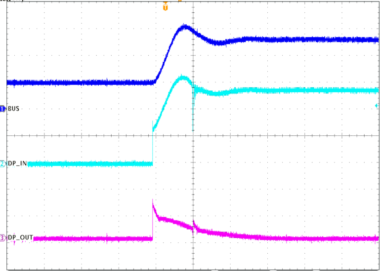
DP_IN/DM_IN shorts to the VBAT protection function, which is realized by the internal protection circuit and external capacitance, C3 (see Figure 2-5). When DP_IN/DM_IN shorts to VBAT, some voltage spikes are clamped by an internal protection circuit, and the other part is absorbed by the external C3 through the internal diode Z1 or Z2. At the same time, output capacitance C4 and C2 are also charged to effectively absorb voltage spikes. Figure 2-6 shows the test results.
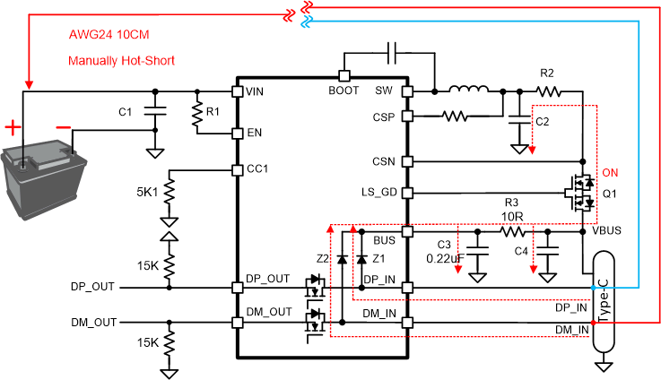
GUID-6A8C3E3D-F187-49BD-87E0-189791509EC0-low.gifFigure 2-5 Power On DP_IN/DM_IN Short-to-VBAT Test Setup
GUID-4C30C399-0A01-4D35-A060-8662528092F9-low.png
CH1 = 5 V/div, CH2 = 5 V/div, CH3 = 5 V/div, 1 µS/div
Figure 2-6 Power On DP_IN Short-to-VBAT Test