SLVAEW7 September 2020 ADC12DJ5200RF , LMK00304 , LMK04828 , LMX2594 , TPS62912 , TPS62913
1.2 Block Diagram
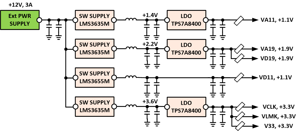
The original ADC12DJ5200 Rev C evaluation module used several SMPS with LDO followers to provide power to the ADC and clock rails. The 3.3V clock rails require low phase noise and low jitter. The 1.1 V analog rail (VA11) requires a separate LDO for the low noise requirements, while the 1.9 V analog and digital rails (VA19 and VD19) is supplied by a single supply as shown in Figure 1-4.
 Figure 1-4 Original Power Block Diagram for ADC12DJ5200 Rev C Evaluation Module
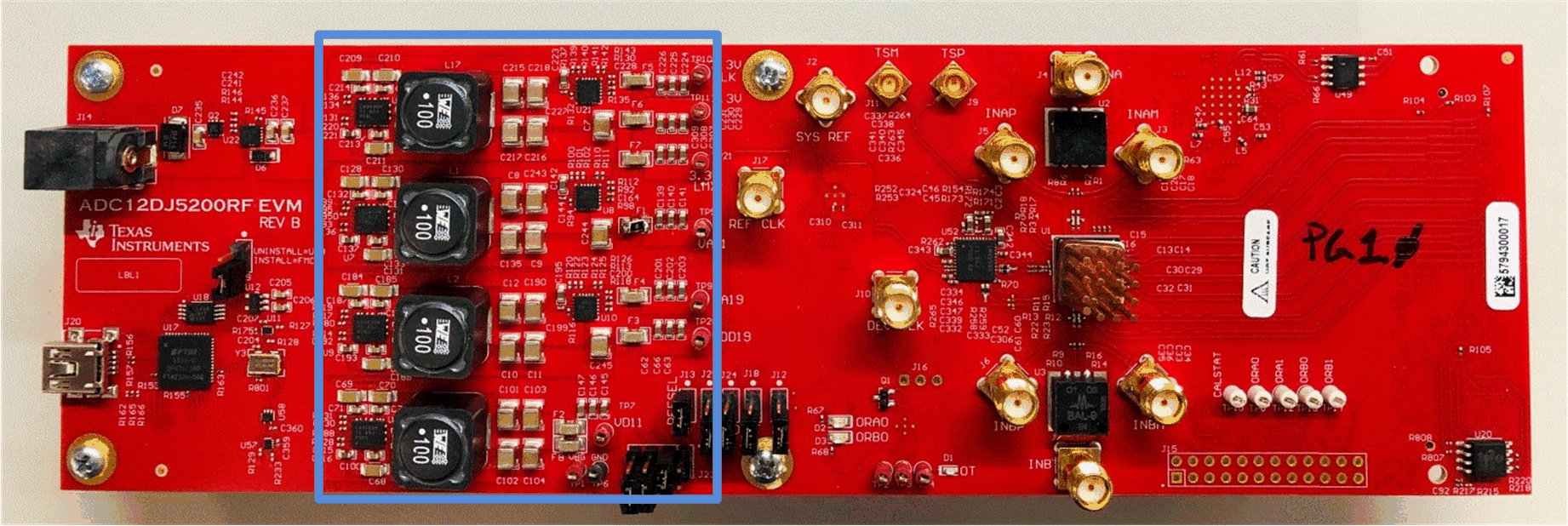
The original EVM power supply is outlined in blue and shown in Figure 1-5.
 Figure 1-5 Image of board with Switchers and LDO's outlined in Blue
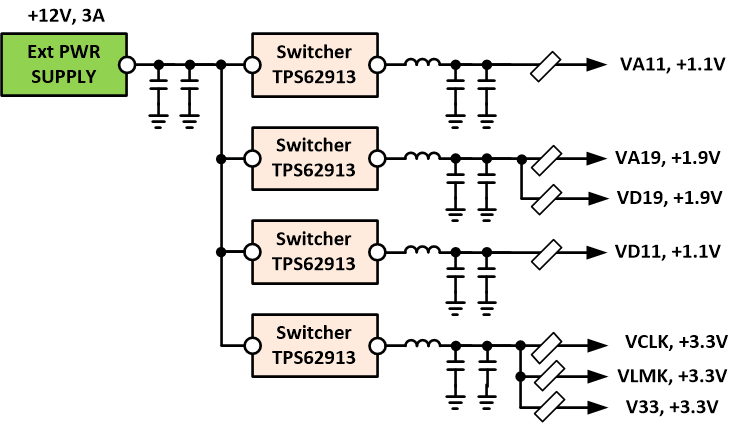
In the revised design, the LDOs are removed and the TPS62913 low-ripple, low-noise SMPS is used instead. This design presents a simplified power supply network for the ADC, where all three power domains are supplied from a DC/DC regulator, with a separate supply for the 3.3-V clock, as shown in Figure 1-6. This implementation improves the efficiency and reduces the part count in comparison to a solution using LDOs while maintaining the output voltage ripple and noise requirements of the ADC and clock for good performance.
 Figure 1-6 Power Block Diagram for ADC12DJ5200 Rev C Evaluation Module with TPS62913
The updated EVM power supply with the TPS62913 is outlined in blue and shown in Figure 1-7.
 Figure 1-7 Image of board with TPS62913 Switchers outlined in Blue
The schematics for the 3.3-V, 1.1-V, and 1.9-V rails can be found in the Section 5.
| Component | Original Rev C | Rev C with TPS62913 |
|---|---|---|
| Switching Power Supplies | 4 x LMS3635M (4mm x 5mm ea) | 4 x TPS62913 (2mm x 2mm ea) |
| LDO's | 3 x TPS7A8400 (3.5mm x 3.5mm ea) | None |
| Size of Power Supplies | 116.75 sqmm + passives | 16 sqmm + passives |