SNOAA61A October 2020 – February 2021 LMG3422R030 , LMG3422R050 , LMG3425R030 , LMG3425R050
4.2 Thermal Simulation Results
The steady-state FEA thermal simulations were
performed with a loss dissipation of 10 W applied on the power device and a constant
temperature of 30 °C set on coldplate. It was assumed that the heat generated by device
only transfers downward to the coldplate through conduction and there is no heat removal
by convection or radiation mechanisms in this thermal model. The system temperature
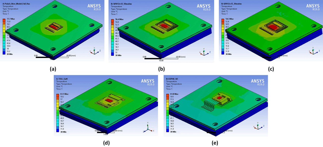
distributions of all investigated package models are illustrated in Figure 4-4. The temperature at
different nodes shown in the Rθ circuit model
(Figure 3-1) can be obtained
from these simulation results and used for thermal resistance calculation between
different nodes. For example, the RθJC/P was calculated using the Equation 3 shown below:
 Figure 4-4 Simulation Results of Temperature Distribution for Different Packages: (a) QFN 8x8, (b) QFN 12x12 (50 mΩ), (c) QFN 12x12 (30 mΩ), (d) TOLL, and (e) D2PAK
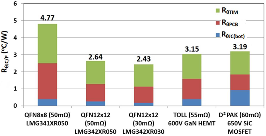
 Figure 4-5 Comparison of Rθ Simulation Results for Different Surface-Mount Packages
Based on the thermal simulation results, Figure 4-5 presents the calculated RθJC/P values for different products packaged in various formats. It is clearly demonstrated that for the same 50-mΩ on-resistance device the RθJC/P of QFN 12x12 package (2.64 °C/W) decreases more than 40% compared to that of QFN 8x8 package (4.77 °C/W). The 30-mΩ device in the same QFN 12x12 package performs slightly better than the 50-mΩ one mainly because the die size is larger for the lower on-resistance device. From the Rθ breakdown analysis also shown in Figure 4-5, it can be observed that the reduction of RθJC/P for QFN 12x12 package compared to its QFN 8x8 predecessor is mostly attributed to the decrease of RθPCB and RθTIM. Such thermal performance improvement is realized by taking advantage of its larger thermal pad and package size which enables the use of a thermally more effective Cu mounting pad and more thermal vias in PCB design. Comparing with other bottom-side cooled, surface-mount packages (i.e., TOLL and D2PAK) used for discrete power devices, QFN 12x12 package has a lower RθJC/P by about 16%, showing its thermal advantage.