SNVA951 November 2020 LM61460-Q1 , LM63615-Q1 , LM63625-Q1 , LM63635-Q1 , LMR33620-Q1 , LMR33630-Q1
4 Package Type
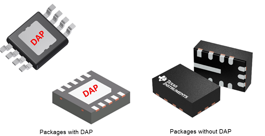
The type of package has a major impact on the thermal performance. In this discussion packages are divided into two major groups: those that have a Die Attach Paddle (DAP) on the bottom of the package and those that do not. Of course there are many more distinctions between packages and many other important features, but this difference is the most important from a thermal perspective. As an example, the LMR33630 is available in both an HSOIC and flip-chip (or HotRod™) QFN package, as Figure 4-1 shows.
 Figure 4-1 LMR33630-Q1 Package Variants.
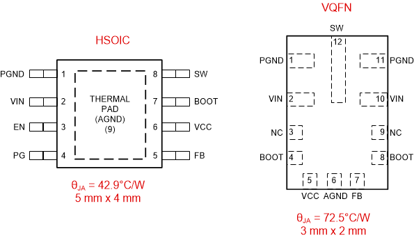
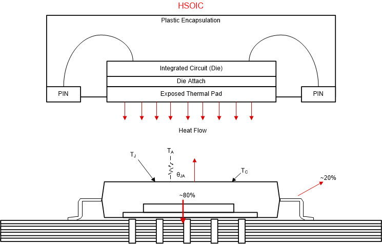
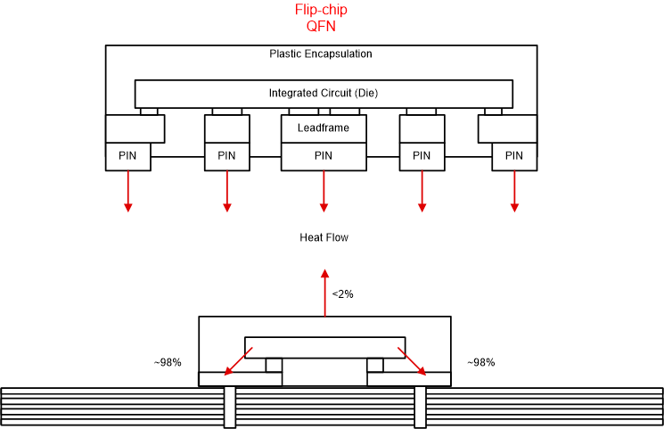
 For this family of devices, Figure 4-2 shows the difference in θJA between the two packages. The values are based on a JEDEC standard board, and it is easy to see that the HSOIC package has a much lower thermal resistance. The tradeoff is also obvious; the HSOIC package is over three times the area of the flip-chip QFN in this example. A QFN package also requires more care in assembly to the PCB than a larger package with completely exposed pins. Figure 4-3 and Figure 4-4 help to explain the difference in thermal resistance between these two example packages. The HSOIC has a large metallic "slug", the DAP, attached directly to the regulator die. The DAP, in turn, is soldered to the PCB copper heat sink. This provides a very low resistance path from the die (heat generator) to the heat sink and outside ambient. As a result, about 80% of the heat flows through the DAP, 20% through the leads, and very little through the plastic. This makes the copper under the DAP (usually electrical ground) very effective in removing the heat from the package.
With the flip-chip package the back-side of the die (or substrate) is facing up, away from the PCB. The only metallic connection to the PCB is through the package pins. This forces the heat to flow through a very restricted path and increases the effective thermal resistance. It also indicates that the copper paths to the pins should be as substantial as possible to help act as a heat sink. For a DC/DC converter the VIN, GND, and SW pins are the most effective in removing the heat, and should be made wide.
Of course these are only two examples of the types of power packages available to the designer. TI offers many package types that provide the advantages of both good thermal performance and small size. An example is the automotive qualified LM63635-Q1. This device is offered in a small 3.00-mm by 3.00-mm WSON package with a DAP; giving comparable performance to a much larger package.
Remember that the JEDEC standard board overemphasizes the difference between the flip-chip QFN and the HSOIC. In many real applications, values of overall θJA can be made comparable between these two packages. For the flip-chip QFN, more PCB copper area will be required, than for a package with a DAP. In any case, as previously stated, the values of θJA given in the table would not be used for design purposes.
 Figure 4-2 Comparison of HSOIC and VQFN Performance.
  Figure 4-3 Typical Heat Flow in HSOIC Package.
  Figure 4-4 Typical Heat Flow in VQFN Package.