SNVA951 November 2020 LM61460-Q1 , LM63615-Q1 , LM63625-Q1 , LM63635-Q1 , LMR33620-Q1 , LMR33630-Q1
6 PCB Layout Tips
In addition to the considerations given in the previous section, there are a few more details that should be kept in mind. The regulator can be considered as a "point" source of heat, when compared to the surrounding PCB. As shown in Figure 6-1, the heat will propagate radially from this source. You can think of the heat flow as a "pizza" slice, as shown in the figure. In our case the heat is flowing along the copper plane of the PCB. It is important not to obstruct this radial path to achieve good thermal performance.
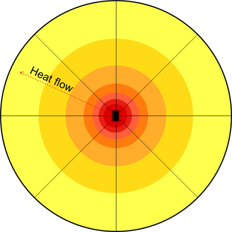 Figure 6-1 Heat Flow in "Pizza"
Slice.
 Two important points can be learned from this model. First, the "tip" of the slice should be well connected to the heat source so that the entire slice is effective in providing a heat sink. That means avoiding cuts in the thermal plane near the device. It also means trying to put non-critical components on the side opposite the heat generating source. Secondly, it is not possible to completely avoid breaking up the thermal plane, since connections must be made to the regulator, along with critical external components. This model shows that the cuts should be made as radially as possible. Figure 6-2 shows an example of both good and bad practices.
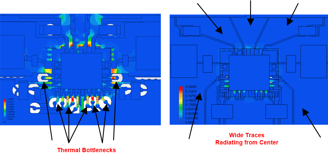 Figure 6-2 Comparison of Heat Flow
Between Two PCB Layouts.
 This theme is continued in the example layout for the LMR33630-Q1, in the flip-chip package, shown in Figure 6-3. This shows a similar strategy of fat, wide traces radiating from the center.
Another aspect of good thermal design is how to deal with more than one heat generating source. For a switching regulator both the converter and the inductor will be dissipating power. Good electrical design usually dictates that these components are placed in close proximity to each other. It turns out that placing heat producing components too close together can have a larger effect on thermal performance than one would think. A heat generating component will have a "thermal footprint" that is about 18 times the area of the component package, as shown in Figure 6-4. A thermal footprint is the area of the PCB that participates strongly in the radiation and convection of the package. If these footprints are allowed to overlap, there will be a drastic increase in component temperature. The effect is most significant when the packages get closer than about twice the package dimension. Figure 6-5 shows measured data demonstrating this non-linear effect.
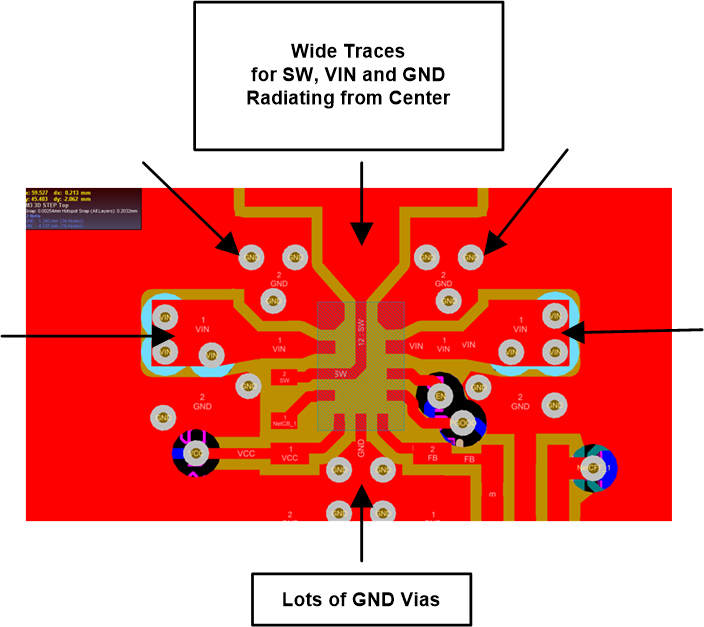 Figure 6-3 LMR3363-Q1 RNX PCB Layout
Example for Good Thermal Performance.
 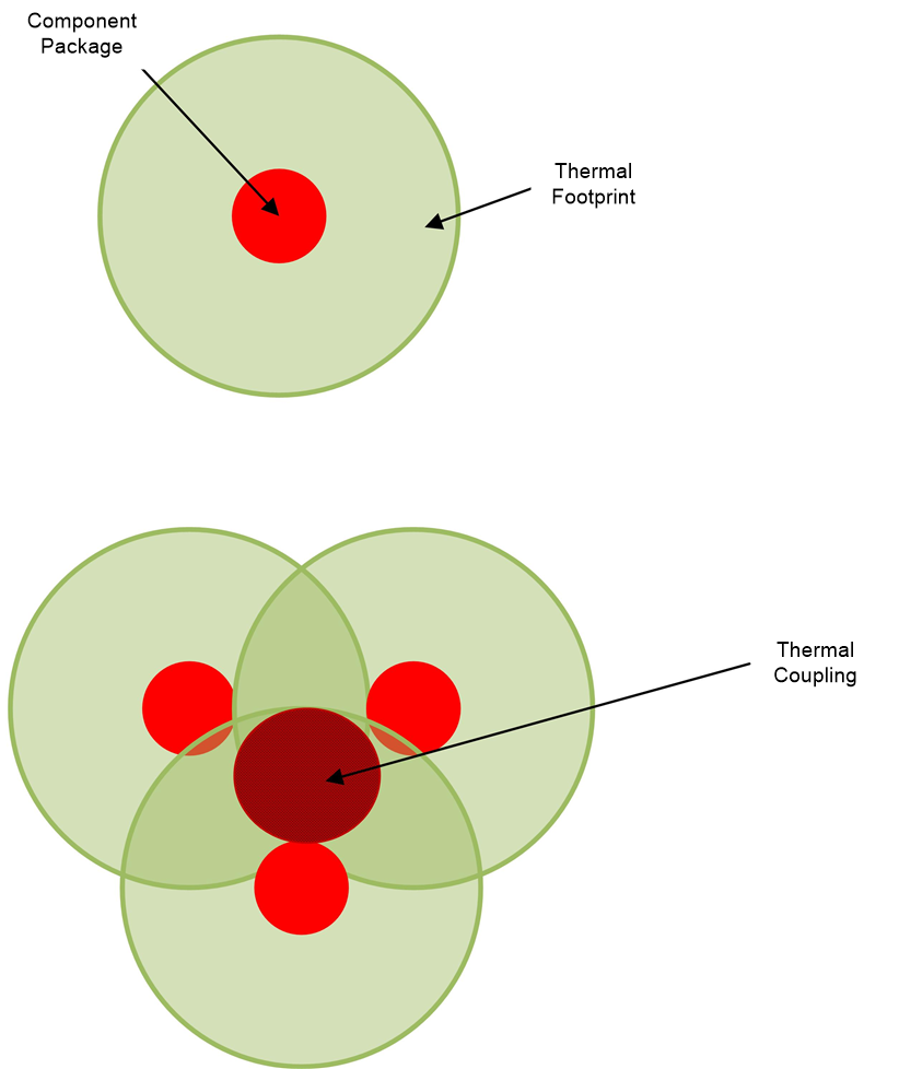 Figure 6-4 Example of Thermal Footprint
Concept.
 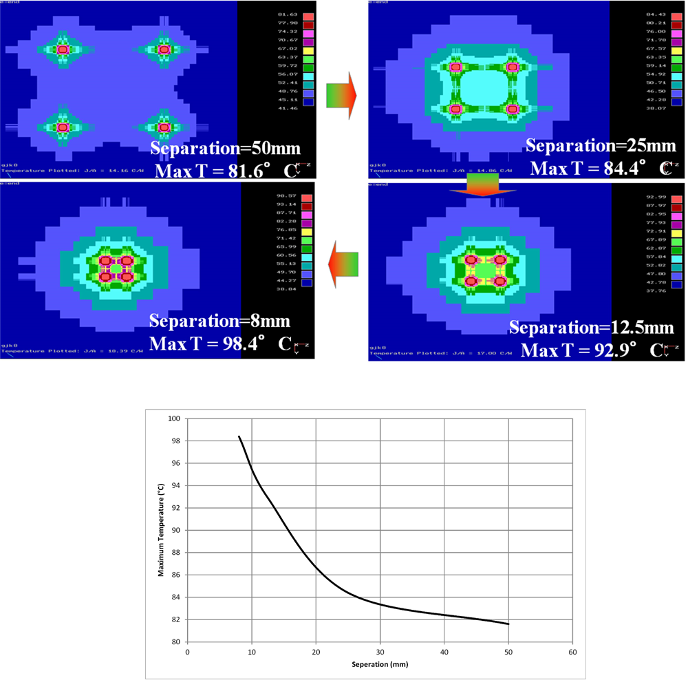 Figure 6-5 Measurement Showing the Effect
of Component Crowding.
 Keep in mind that thermal considerations are not the only ones that enter into a good PCB layout for a DC/DC converter. Certain critical components need to be close to and on the same side as the converter. Also, wide traces on the switch node may aggravate EMI issues. The converter inductor also dissipates substantial power. However, it usually will need to be close to the device to minimize switch node area. In other words a compromise must be found; just as with any good engineering design. The best resource for good overall PCB design can be found in the regulator data sheet, and the recommendations found there should always be followed. Table 6-1 gives a summary of some best practices for good thermal PCB layout.
| Use a package with a DAP | If this option is available, it makes it easier to reduce the overall θJA and achieve the target thermal performance. |
| Maximize the copper layer on the same side as the device. | This layer will usually be ground and acts as the most effective heat sink for the device. |
| Use the thickest copper allowable. | Thick copper affords lower thermal resistance. |
| Widen PCB traces near the device. | Wide traces afford lower thermal resistance. |
| Avoid breaks in heat flow | Use the "pizza" slice concept when routing copper layers. |
| Judicial use of thermal vias | Use enough vias to connect the copper planes together to help reduce thermal resistance. Especially true under the DAP. |
| Avoid crowding together heat producing sources | Keep in mind the thermal footprint of heat generating sources such as the inductor when planning the PCB layout. |