SPRAAV1C May 2009 – March 2020 AM3703 , AM3715 , OMAP3503 , OMAP3515 , OMAP3525 , OMAP3530
-
PCB Design Guidelines for 0.4mm Package-On-Package (PoP) Packages, Part I
- Trademarks
- 1 Using This Guide
- 2 A Word of Caution
- 3 A Team Sport
- 4 Be Wary of Quotes
- 5 Don’t Forget Your CAD Tools
- 6 Metric Vs English
- 7 PCB Fab Limits
- 8 Routing and Layer Stackup
- 9 OMAP35x 0.4mm Pitch
- 10 Pad Type
- 11 PCB Pad Dimensions for 0.4mm BGA Package
- 12 Multiple BGA Packages
- 13 Etch Traps and Heat Sinks
- 14 Vias and VIP
- 15 Laser Blind Vias
- 16 Filled Vias
- 17 Know Your Tools
- 18 BeagleBoard
- 19 BeagleBoard Views
- 20 OMAP35x Decoupling
- 21 PCB Finishes for High Density Interconnect (HDI)
- 22 Real World Second Opinion
- 23 Acknowledgments
- 24 References
- Revision History
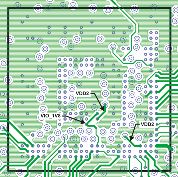
19.2 Layer 2 – Ground
The ground plane is the shaded green area.
 Figure 20. Close-Up of BeagleBoard Layer 2 - Ground Plane