SPRAAV1C May 2009 – March 2020 AM3703 , AM3715 , OMAP3503 , OMAP3515 , OMAP3525 , OMAP3530
-
PCB Design Guidelines for 0.4mm Package-On-Package (PoP) Packages, Part I
- Trademarks
- 1 Using This Guide
- 2 A Word of Caution
- 3 A Team Sport
- 4 Be Wary of Quotes
- 5 Don’t Forget Your CAD Tools
- 6 Metric Vs English
- 7 PCB Fab Limits
- 8 Routing and Layer Stackup
- 9 OMAP35x 0.4mm Pitch
- 10 Pad Type
- 11 PCB Pad Dimensions for 0.4mm BGA Package
- 12 Multiple BGA Packages
- 13 Etch Traps and Heat Sinks
- 14 Vias and VIP
- 15 Laser Blind Vias
- 16 Filled Vias
- 17 Know Your Tools
- 18 BeagleBoard
- 19 BeagleBoard Views
- 20 OMAP35x Decoupling
- 21 PCB Finishes for High Density Interconnect (HDI)
- 22 Real World Second Opinion
- 23 Acknowledgments
- 24 References
- Revision History
11 PCB Pad Dimensions for 0.4mm BGA Package
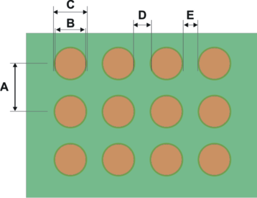
Through several meetings with both board fabricators and board assembly houses, the following recommendation has been created for the circuit board BGA footprint for the OMAP35x having 0.4mm or 400 μm, pitch solder balls. Figure 8 shows the top layer with vias down to layer 2.
At the 0.4mm pitch, there is insufficient space between pads to allow a 3mil trace to run between pads without incurring solder bridging. Therefore, except for the outside perimeter balls, all connections are routed to the lower layers through VIP technology. With this technology, only six layers were needed for the BeagleBoard.
For the BeagleBoard design, the desired finished pad size is equal to the solder ball diameter. Since no traces run between the pads, the copper pad is enlarged to 280 μm (11mils). The solder mask opening is set to 254 μm (10 mils).
With this arrangement, there is plenty of solder webbing between pads which helps prevent adjacent ball solder bridging. For more information regarding additional parameters that impact the assembly of this package, see PCB Assembly Guidelines for 0.4mm Package-On-Package (PoP) Packages, Part II.
| Pad Type | Solder Mask Defined | |
| Pad Pitch | A | 400 μm (0.4mm) |
| Mask Opening | B | 254 μm (10 mils) |
| Pad Size | C | 280 μm (11 mils) |
| Mask Shape | Round | |
| Mask Web | D | 150 μm |
| Pad to Pad Clearance | E | 120 μm |
| Trace Allowed Between | No |
 Figure 8. Recommendations for 0.4mm Pitch Packages - Top Layer