SPRAAV1C May 2009 – March 2020 AM3703 , AM3715 , OMAP3503 , OMAP3515 , OMAP3525 , OMAP3530
-
PCB Design Guidelines for 0.4mm Package-On-Package (PoP) Packages, Part I
- Trademarks
- 1 Using This Guide
- 2 A Word of Caution
- 3 A Team Sport
- 4 Be Wary of Quotes
- 5 Don’t Forget Your CAD Tools
- 6 Metric Vs English
- 7 PCB Fab Limits
- 8 Routing and Layer Stackup
- 9 OMAP35x 0.4mm Pitch
- 10 Pad Type
- 11 PCB Pad Dimensions for 0.4mm BGA Package
- 12 Multiple BGA Packages
- 13 Etch Traps and Heat Sinks
- 14 Vias and VIP
- 15 Laser Blind Vias
- 16 Filled Vias
- 17 Know Your Tools
- 18 BeagleBoard
- 19 BeagleBoard Views
- 20 OMAP35x Decoupling
- 21 PCB Finishes for High Density Interconnect (HDI)
- 22 Real World Second Opinion
- 23 Acknowledgments
- 24 References
- Revision History
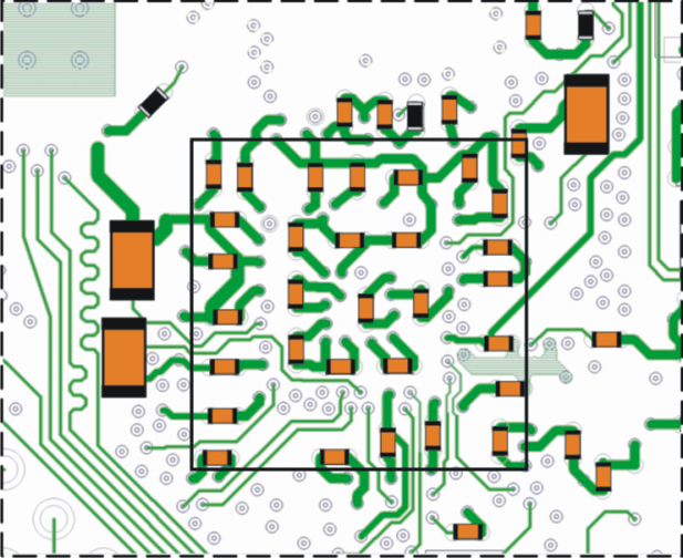
19.6 Layer 6 – Signal – Bottom Copper – Bottom Component Outlines
The bottom layer view has been enlarged in scope to show more of the board and to show most of the OMA35xx supply bypass capacitors (shown in orange.) The two small black colored items are resistors.
The X7R bypass capacitors are the smaller 0402 packages and are all rated at 0.1μF/10 V. The three larger capacitors are all 1μF and are used to bypass the OMAP3 processor’s internally derived voltages and references.
 Figure 24. Close-Up of BeagleBoard Layer 6 - Bottom Side