SPRABA5D January 2014 – January 2019 AM1802 , AM1802 , AM1806 , AM1806 , AM1808 , AM1808 , AM1810 , AM1810
-
Using the AM18xx Bootloader
- Trademarks
- 1 Introduction
- 2 Boot Modes
- 3 Non-AIS Boot Modes
- 4
Application Image Script (AIS) Boot
- 4.1 Section Load Command (0x58535901)
- 4.2 Section Fill Command (0x5853590A)
- 4.3 Enable CRC Command (0x58535903)
- 4.4 Disable CRC Command (0x58535904)
- 4.5 Validate CRC Command (0x58535902)
- 4.6 Jump & Close Command (0x58535906)
- 4.7 Jump Command (0x58535905)
- 4.8 Sequential Read Enable Command (0x58535963)
- 4.9 Function Execute Command (0x5853590D)
- 4.10 Boot Table Command (0x58535907)
- 5
AISgen: Tool to Generate Boot Script (AIS Image)
- 5.1 Installation
- 5.2 Getting Started
- 5.3
Generating AIS
- 5.3.1 Boot Mode and Boot Peripheral Setup
- 5.3.2 Phase-Locked Loop (PLL) Setup
- 5.3.3 Synchronous Dynamic Random Access Memory (SDRAM) Setup
- 5.3.4 DDR Setup
- 5.3.5 PSC Setup
- 5.3.6 Pin Multiplexing Setup
- 5.3.7 Application File Selection
- 5.3.8 AIS File Selection
- 5.3.9 Status and Messages
- 5.3.10 Additional AIS Options
- 5.3.11 Command Line Usage
- 6 Master Boot – Booting From a Slave Memory Device
- 7 Slave Boot – Booting From an External Master Host
- 8 UART Boot Host - Using Your PC as a UART Boot Master
- 9 Boot Requirements, Constraints and Default Settings
- 10 References
- A Boot Mode Selection Table
- B Details of Supported NAND Devices
- C CRC Computation Algorithm
-
D Details of Pre-Defined ROM Functions
- D.1 PLL0 Configuration (Index = 0, Argument Count = 2)
- D.2 PLL1 Configuration (Index = 1, Argument Count = 2)
- D.3 Clock Configuration (Index = 2, Argument Count = 1)
- D.4 mDDR/DDR2 Controller Configuration (Index = 3, Argument Count = 8)
- D.5 EMIFA SDRAM Configuration (Index = 4, Argument Count = 5)
- D.6 EMIFA Async Configuration (Index = 5, Argument Count = 5)
- D.7 PLL and Clock Configuration (Index = 6, Argument Count = 3)
- D.8 Power and Sleep Configuration (PSC) (Index = 7, Argument Count = 1)
- D.9 Pinmux Configuration (Index = 8, Argument Count = 3)
- E ROM Revision History
- Revision History
4.10 Boot Table Command (0x58535907)
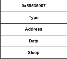
The Boot Table (or SET) command writes 8-, 16-, or 32-bit data to any address in device memory. Additionally, it instructs the device to wait for a fixed number of cycles after the memory write occurs. This can allow memory-mapped register writes to take effect before the bootloader moves on to the next opcode.
 Figure 18. Boot Table Command
 This command takes four arguments. First is the type (size and format) of the memory location to be written; the contents of this word are described in the table below. The address comes next, followed by the data. Note that the data is given as 32 bits in the AIS regardless of how many bits will actually be written. The last parameter is the number of cycles to delay execution of the next opcode.
| 31 | 24 | 23 | 16 | 15 | 8 | 7 | 0 |
| Reserved | STOP | START | LENGTH |
| LEGEND: R/W = Read/Write; R = Read only; -n = value after reset |
Table 3. Type Word for Boot Table Opcode Field Descriptions
| Bit | Field | Value | Description |
|---|---|---|---|
| 31-24 | Reserved | 0 | Reserved |
| 23-16 | STOP | 0-31 | The highest (or most significant) bit of the custom data field. Only used when LENGTH = 3 or 4. |
| 15-8 | START | 0-31 | The lowest (or least significant) bit of the custom data field. Only used when LENGTH = 3 or 4. |
| 7-0 | LENGTH | Size of data word | |
| 0 | 8-bit | ||
| 1 | 16-bit | ||
| 2 | 32-bit | ||
| 3-4 | Custom field defined by STOP, START. Data outside this field at the target address will be preserved. | ||
| 5-FFhC | Reserved |