SPRABA5D January 2014 – January 2019 AM1802 , AM1802 , AM1806 , AM1806 , AM1808 , AM1808 , AM1810 , AM1810
-
Using the AM18xx Bootloader
- Trademarks
- 1 Introduction
- 2 Boot Modes
- 3 Non-AIS Boot Modes
- 4
Application Image Script (AIS) Boot
- 4.1 Section Load Command (0x58535901)
- 4.2 Section Fill Command (0x5853590A)
- 4.3 Enable CRC Command (0x58535903)
- 4.4 Disable CRC Command (0x58535904)
- 4.5 Validate CRC Command (0x58535902)
- 4.6 Jump & Close Command (0x58535906)
- 4.7 Jump Command (0x58535905)
- 4.8 Sequential Read Enable Command (0x58535963)
- 4.9 Function Execute Command (0x5853590D)
- 4.10 Boot Table Command (0x58535907)
- 5
AISgen: Tool to Generate Boot Script (AIS Image)
- 5.1 Installation
- 5.2 Getting Started
- 5.3
Generating AIS
- 5.3.1 Boot Mode and Boot Peripheral Setup
- 5.3.2 Phase-Locked Loop (PLL) Setup
- 5.3.3 Synchronous Dynamic Random Access Memory (SDRAM) Setup
- 5.3.4 DDR Setup
- 5.3.5 PSC Setup
- 5.3.6 Pin Multiplexing Setup
- 5.3.7 Application File Selection
- 5.3.8 AIS File Selection
- 5.3.9 Status and Messages
- 5.3.10 Additional AIS Options
- 5.3.11 Command Line Usage
- 6 Master Boot – Booting From a Slave Memory Device
- 7 Slave Boot – Booting From an External Master Host
- 8 UART Boot Host - Using Your PC as a UART Boot Master
- 9 Boot Requirements, Constraints and Default Settings
- 10 References
- A Boot Mode Selection Table
- B Details of Supported NAND Devices
- C CRC Computation Algorithm
-
D Details of Pre-Defined ROM Functions
- D.1 PLL0 Configuration (Index = 0, Argument Count = 2)
- D.2 PLL1 Configuration (Index = 1, Argument Count = 2)
- D.3 Clock Configuration (Index = 2, Argument Count = 1)
- D.4 mDDR/DDR2 Controller Configuration (Index = 3, Argument Count = 8)
- D.5 EMIFA SDRAM Configuration (Index = 4, Argument Count = 5)
- D.6 EMIFA Async Configuration (Index = 5, Argument Count = 5)
- D.7 PLL and Clock Configuration (Index = 6, Argument Count = 3)
- D.8 Power and Sleep Configuration (PSC) (Index = 7, Argument Count = 1)
- D.9 Pinmux Configuration (Index = 8, Argument Count = 3)
- E ROM Revision History
- Revision History
5.3.4 DDR Setup
The DDR tab appears when the Configure DDR checkbox is selected. This tab configures external DDR memory access through the DDR Controller. The DDR Controller registers need to be configured before any access to DDR is made. The DDR controller can be configured to access DDR2 or mDDR memory. Certain registers are only used for mDDR.
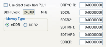
Values entered for each DDR register are directly programmed to the corresponding register by the bootloader. The Use direct clock from PLL1 checkbox allows the DDR Controller to use the output of PLL1 before the post divider is applied. The DDR clock field displays the calculated clock speed for DDR access, and is the same as the identical field in the PLL1 tab.