SPRABA5D January 2014 – January 2019 AM1802 , AM1802 , AM1806 , AM1806 , AM1808 , AM1808 , AM1810 , AM1810
-
Using the AM18xx Bootloader
- Trademarks
- 1 Introduction
- 2 Boot Modes
- 3 Non-AIS Boot Modes
- 4
Application Image Script (AIS) Boot
- 4.1 Section Load Command (0x58535901)
- 4.2 Section Fill Command (0x5853590A)
- 4.3 Enable CRC Command (0x58535903)
- 4.4 Disable CRC Command (0x58535904)
- 4.5 Validate CRC Command (0x58535902)
- 4.6 Jump & Close Command (0x58535906)
- 4.7 Jump Command (0x58535905)
- 4.8 Sequential Read Enable Command (0x58535963)
- 4.9 Function Execute Command (0x5853590D)
- 4.10 Boot Table Command (0x58535907)
- 5
AISgen: Tool to Generate Boot Script (AIS Image)
- 5.1 Installation
- 5.2 Getting Started
- 5.3
Generating AIS
- 5.3.1 Boot Mode and Boot Peripheral Setup
- 5.3.2 Phase-Locked Loop (PLL) Setup
- 5.3.3 Synchronous Dynamic Random Access Memory (SDRAM) Setup
- 5.3.4 DDR Setup
- 5.3.5 PSC Setup
- 5.3.6 Pin Multiplexing Setup
- 5.3.7 Application File Selection
- 5.3.8 AIS File Selection
- 5.3.9 Status and Messages
- 5.3.10 Additional AIS Options
- 5.3.11 Command Line Usage
- 6 Master Boot – Booting From a Slave Memory Device
- 7 Slave Boot – Booting From an External Master Host
- 8 UART Boot Host - Using Your PC as a UART Boot Master
- 9 Boot Requirements, Constraints and Default Settings
- 10 References
- A Boot Mode Selection Table
- B Details of Supported NAND Devices
- C CRC Computation Algorithm
-
D Details of Pre-Defined ROM Functions
- D.1 PLL0 Configuration (Index = 0, Argument Count = 2)
- D.2 PLL1 Configuration (Index = 1, Argument Count = 2)
- D.3 Clock Configuration (Index = 2, Argument Count = 1)
- D.4 mDDR/DDR2 Controller Configuration (Index = 3, Argument Count = 8)
- D.5 EMIFA SDRAM Configuration (Index = 4, Argument Count = 5)
- D.6 EMIFA Async Configuration (Index = 5, Argument Count = 5)
- D.7 PLL and Clock Configuration (Index = 6, Argument Count = 3)
- D.8 Power and Sleep Configuration (PSC) (Index = 7, Argument Count = 1)
- D.9 Pinmux Configuration (Index = 8, Argument Count = 3)
- E ROM Revision History
- Revision History
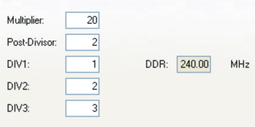
5.3.2 Phase-Locked Loop (PLL) Setup
When the device is taken out of reset, the PLL modules are set in bypass mode by default. During application development, the PLL configuration is typically handled by a GEL file. In a production environment, the bootloader can configure the PLL. The AISgen General tab specifies the clock source and its frequency, and the PLL0 and PLL1 tabs can configure the multipliers and dividers to reach the desired CPU frequency.
The PLL0 tab appears when the Configure PLL0 checkbox is selected. This tab configures the multiplier and dividers for PLL0. When changing any of these values, calculated frequencies will update to reflect the changes. The multiplier and divider values that you enter are the actual multiplication and division factors (x), not the values that get programmed into the corresponding PLL registers (x - 1). The default settings of the PLL dividers that are not configurable are shown in Table 5.
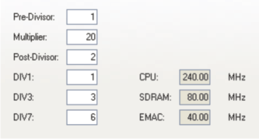
Table 5. Values of Non-User Configurable PLL0 Dividers (relative to DIV1)
| Divider | Configured To |
|---|---|
| PLL0 DIV2 | Divide by 2 |
| PLL0 DIV4 | Divide by 4 |
| PLL0 DIV6 | Divide by 1 |
The PLL1 tab appears when the Configure PLL1 checkbox is selected. Note that PLL1 must be configured if DDR is configured. Selecting the Configure DDR checkbox will automatically select Configure PLL1 as well. This tab is similar to the PLL0 tab, but its settings are applied to PLL1 instead of PLL0.