SPRAD62 February 2023 F29H850TU , F29H859TU-Q1 , TMS320F280023C , TMS320F280025C , TMS320F280025C-Q1 , TMS320F280037C , TMS320F280037C-Q1 , TMS320F280038C-Q1 , TMS320F280039C , TMS320F280039C-Q1 , TMS320F28386D , TMS320F28386D-Q1 , TMS320F28386S , TMS320F28386S-Q1 , TMS320F28388D , TMS320F28388S , TMS320F28P650DH , TMS320F28P650DK , TMS320F28P650SH , TMS320F28P650SK , TMS320F28P659DH-Q1 , TMS320F28P659DK-Q1 , TMS320F28P659SH-Q1
- Abstract
- Trademarks
- 1Introduction
- 2Serial Port Design Methodology
- 3Example A: Using the CLB to Input and Output a TDM Stream in Audio Applications
- 4Example B: Using the CLB to Implement a Custom Communication Bus for LED Driver in Lighting Applications
- 5References
3.7.3 Testing Output Setup and Hold Times
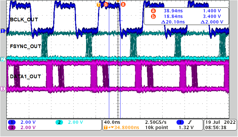
A key consideration in the output TDM stream from the CLB is the expected setup and hold time seen by the receiving device. To measure the setup and hold time, an oscilloscope was used to continuously capture the output of the CLB. Figure 3-15 shows the TDM output without the latch and delay logic added to the FSYNC_OUT and DATA1_OUT signals. The setup and hold time of DATA1_OUT with respect to BCLK_OUT reduced due to the delay in the DATA1_OUT signal.
 Figure 3-15 TDM-8 Output Without Latch and
Delay Logic
Figure 3-15 TDM-8 Output Without Latch and
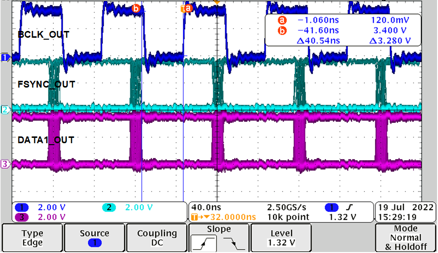
Delay LogicThe oscilloscope plot shown in Figure 3-16 shows the final TDM output with the latch and delay logic added to the FSYNC_OUT and DATA1_OUT signals. The setup and hold time are greatly improved using this approach.
 Figure 3-16 Final TDM-8 Output
Since BCLK_OUT must be passed through the CLB tile without jitter, it is not possible to accurately control the timing between BCLK_OUT and the other two signals without introducing jitter on BCLK_OUT. However, in this case, the setup and hold time are acceptable. If needed the BCLK_OUT signal can be inverted using the AOC in the CLB tile to trade setup for hold time.
Finally note the 10 ns jitter on the FSYNC_OUT and DATA1_OUT signals. This is due to the CLB tile sampling the incoming BCLK_IN signal at 100 MHz. The jitter reduces the setup and hold time further.