SPRUIT1B May   2020  – November 2020


  1.   Trademarks
  2. 1Introduction
    1. 1.1 Key Features
  3. 2GESI Expansion Board Overview
    1. 2.1 GESI Expansion Board Identification
    2. 2.2 GESI Expansion Board Component Identification
  4. 3GESI Expansion Board - User Setup/Configuration
    1. 3.1 GESI Infotainment Expansion Board With CP Board
      1. 3.1.1 Board Assembly Procedures
    2. 3.2 Power Requirements
    3. 3.3 EVM Reset/Interrupt Push Buttons
    4. 3.4 EVM Configuration DIP Switch
  5. 4GESI Expansion Board Hardware Architecture
    1. 4.1  GESI Expansion Board Hardware Top Level Diagram
    2. 4.2  Expansion Connectors
    3. 4.3  Board ID EEPROM
    4. 4.4  Ethernet Interface
      1. 4.4.1 RGMII Clocking Scheme
      2. 4.4.2 Ethernet Port LED Indication
    5. 4.5  PROFI BUS / RS485
    6. 4.6  LIN Interface
    7. 4.7  MCAN
    8. 4.8  MUX Selection
      1. 4.8.1 MUX – PRGx_MDIO/MDC, CPSW9G_MDIO/MDC
      2. 4.8.2 MUX – PRG1_RGMII1/PRG1_PWM
      3. 4.8.3 MUX – PRG1_PWM/MCAN
      4. 4.8.4 MUX_MC/BP_SEL
    9. 4.9  GESI LaunchPad-Booster Pack Interface
    10. 4.10 Motor Control Interface
    11. 4.11 USS/IMU Header
    12. 4.12 Test Header
  6.   A Interface Mapping
  7.   B GESI Board GPIO Mapping
  8.   C I2C Address Mapping
  9.   D Revision History

GESI Expansion Board Hardware Top Level Diagram

Figure 4-1 shows the functional block diagram of the GESI expansion board
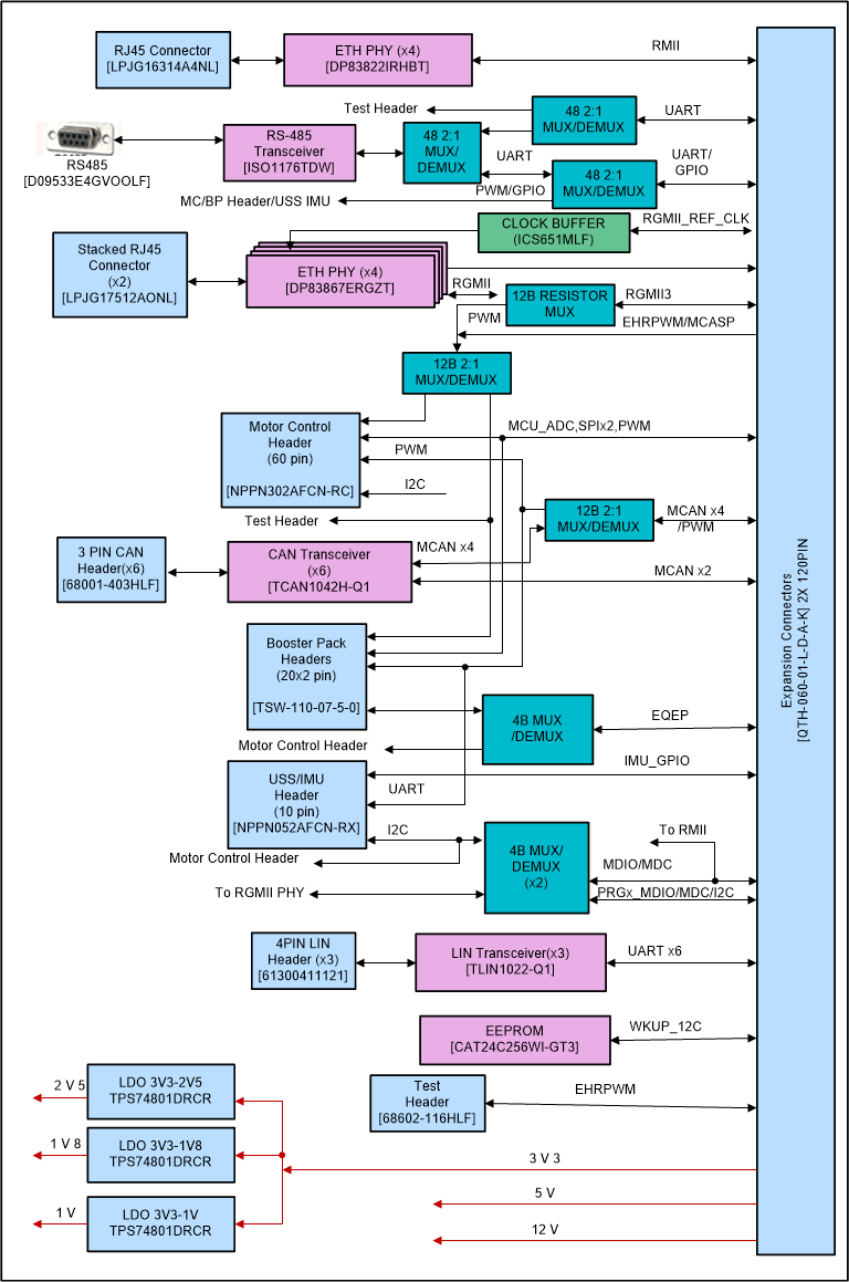
GUID-DC972686-6F64-41E4-8E62-B4893928CF2D-low.gifFigure 4-1 Functional Block Diagram of Infotainment Expansion Board

Few of the interfaces shown in the above diagram are specific EVM dependency. All may not be supported in all the Jacinto7 EVM.

For supported interfaces on the specific EVM platform, see Section A.