SWRA729 April   2022 CC1352P , CC2652P


  1.   Trademarks
  2.   Acronyms
  3. 1Reference Designs Available
    1. 1.1 Single Component for 10-dBm PA Port
      1. 1.1.1 Murata PA IPC Equivalent Circuit
      2. 1.1.2 IPC Size and Dimensions
    2. 1.2 CC2652P PA IPC EM
      1. 1.2.1 Component Placement and Layout
      2. 1.2.2 Layout - Layer 1
      3. 1.2.3 Layout - Layer 2
      4. 1.2.4 Layout - Layer 3
      5. 1.2.5 Layout - Layer 4
  4. 2PA IPC Measurement Results
    1. 2.1 CC2652P Output Power, 1-Mbps Bluetooth Low Energy
    2. 2.2 CC2652P TX Efficiency, Harmonics, and Output Power at Various PA Settings
  5. 3Harmonic Emission Regulatory Requirements
    1. 3.1 Compliance with FCC regulations
    2. 3.2 Compliance with Regulations
  6. 4Summary
  7. 5References

Layout - Layer 2

Figure 1-8 shows the second layer of the 4-layer reference design. This layer is mainly a GND layer. It is important to have a solid ground plane underneath the complete RF section and to avoid any routing directly underneath the RF section. The reference design [6] has a thickness of 175 um between layer 1 and layer 2. This is the main parameter in the FR4 PCB stack-up that should be kept similar when copying the reference design.
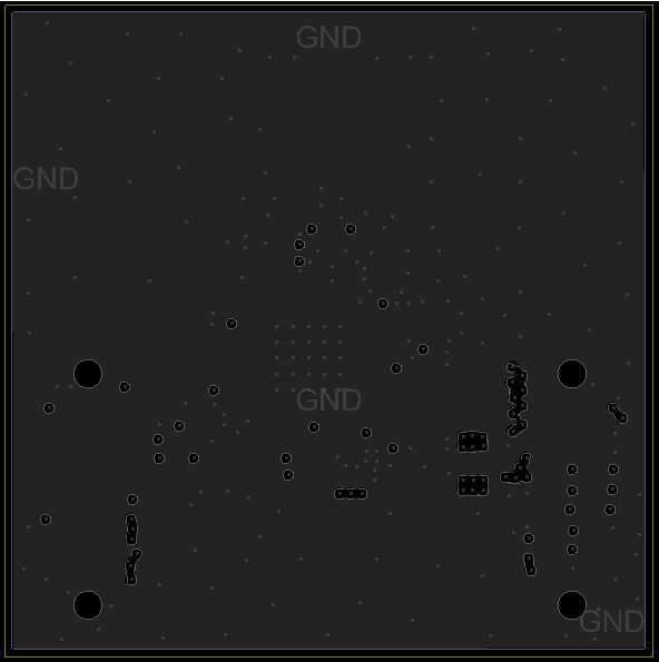
GUID-20211124-SS0I-R3FM-BWD7-TT13BDLFT07P-low.pngFigure 1-8 Layer 2